
User`s manual
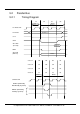

5.1 Definition
The definition of I/O expansion bus is given as follows:
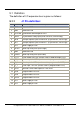
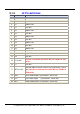
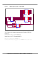
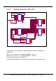
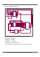
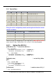
5.1.1 J1 Pin definition:
No Name Description
1 GND Ground of PCB
2 GND Ground of PCB
3 CLOCKA Synchronous clock output of CPU
4 ARDY Asynchronous ready input (level sensitive, OPEN=ready)
5 INT0 Interrupt request input of channel 0 (asynchronous, active high)
6 INT1 Interrupt request input of channel 1 (asynchronous, active high)
7 VCC Power supply of PCB
8 RESET Power up reset pulse (active high)
9 GND Ground of PCB
10 /RESET Power up reset pulse (active low)
11 TO_0 Timer output 0 of CPU (can be used as programmable D/I/O)
12 TO_1 Timer output 1 of CPU (can be used as programmable D/I/O)
13 TI_0 Timer input 0 of CPU (can be used as programmable D/I/O)
14 TI_1 Timer input 1 of CPU (can be used as programmable D/I/O)
15 SCLK Common serial clock output of 7188 series
16 DIO9 Programmable D/I/O bit
17 DIO4 Programmable D/I/O bit
18 DIO14 Programmable D/I/O bit
19 VCC Power supply of PCB
20 VCC Power supply of PCB
I/O Expansion Bus for 7188X/7188E User’s Manual, Jun/2004 v1.4, 7PH-000-14---21