I/O Expansion Bus for 7188X/7188E User’s Manual Warranty All products manufactured by ICP DAS are warranted against defective materials for a period of one year from the date of delivery to the original purchaser. Warning ICP DAS assume no liability for damages consequent to the use of this product. ICP DAS reserves the right to change this manual at any time without notice. The information furnished by ICP DAS is believed to be accurate and reliable.
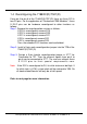
Table of Contents 1. 2. INTRODUCTION............................................................................................. 5 1.1 WHAT IS THE I/O EXPANSION BUS? ............................................................. 5 1.2 1.3 1.4 USING I-7188 I/O EXPANSION BOARDS: ...................................................... 5 OVERVIEW: ................................................................................................ 5 RECONFIGURING THE 7188XC(D)/7521(D) ...........................
7.3 7.4 7.5 8. X002 : PROTOTYPE BOARD ...................................................................... 37 X003: TEST BOARD 1............................................................................... 38 X004: TEST BOARD 2............................................................................... 39 X1XX I/O EXPANSION BOARDS................................................................. 42 8.1 8.2 8.3 8.4 8.5 8.6 8.7 8.8 8.9 8.10 8.11 8.12 9. X100: DI * 8..................................
12. X5XX I/O EXPANSION BOARDS ............................................................. 92 12.1 12.2 12.3 12.4 12.5 12.6 12.7 12.8 12.9 12.10 X500: RS232 * 1 .................................................................................... 92 X501: RS232 * 1 .................................................................................... 95 X502: RS232 * 1 .................................................................................... 96 X503: RS232 * 1 ...................................
1. Introduction 1.1 What is the I/O Expansion Bus? The I-7188XA, I-7188XC, I-7188XB, I-7188XG, I-7188EX, I7188EG & 7521 all support I/O expansion buses. The I/O expansion bus can be used to implement various I/O functions such as D/I, D/O, A/D, D/A, Timer/Counter, UART, flash memory, battery backup SRAM & other I/O functions. Nearly all kinds of I/O functions can be implemented on this bus. 1.2 Using I-7188 I/O Expansion Boards: The I-7188X series can plug an I/O Expansion board inside the main body.
flash memory, battery backup SRAM & other I/O functions. Nearly all kinds of I/O functions can be implemented in this bus. The I/O expansion bus includes serial & parallel interface. The parallel interface is very similar to an ISA bus, so the user can move the old ISA bus design to the I/O expansion bus with very little modification.
The I/O pins of serial bus are programmable. They can be programmed as D/I, or D/O. Some pins can be configured to D/I or D/O or timer input or timer output. There are many serial interface devices today. The features of these serial devices are given as follows: Smaller size compared to parallel devices. Lower cost compared to parallel devices. Easier to design for isolation application. The serial interface of an I/O expansion bus can link to these serial devices very easily.
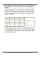
7520 RS232 RS485 Host PC RS485 Standard-7000 RS485 Customized-7000 module (7188X+X???) Standard-7000 Customized-7000 module (7188X+X???) The design of a I/O Expansion Bus make the idea of a“Customized-7000 Module” come true.
1.4 Reconfiguring the 7188XC(D)/7521(D) From pin-4 to pin-8 of the 7188XC(D)/7521(D) there are three D/O & two D/I pins.
Example: The X100 is an 8-channel D/I board designed for the 7188X(D) / 7521(D). It removes all 5 resistors, R19 ~ R23, and reconfigures all these pins as D/I pins. It installs another 5-pin female reconfigurationjumper into TP1 of the 7188XC(D)/7521(D). Therefore, user can select the original 3_DO_2_DI functions or new 5_DI functions by setting the jumper in different positions. The I-7188XB(D), I-7188XG(D), I-7188EX(D), I-7188EG(D) has 14 user-defined pins.
1.5 How to download program under the MiniOS7 ? 1. Create a file folder named "7188X" in your hard drive. For example, "c:\7188X". For Dos, Windows 95 & Windows 98 Users: 2. Copy \Napdos\MiniOS7\utility\7188xw.exe. from the CD_ROM into your "7188X" folder. 3. Run "\7188X\7188xw.exe" in your hard drive. A "7188xw" screen will appear. For Windows NT, Windows 2000 & Windows XP Users: 2. Copy \Napdos\MiniOS7\utility\7188xw.exe. from the CD_ROM into your "7188X" folder. 3. Run "\7188X\7188xw.
9. Power off the I-7188XC controller, connect pin "INIT" to "INIT COM" and then power it up. 10. Type "del" and reply "y" to delete the current driver. 7188x> del Total File number is 2, do you really want to delete(y/n)? 11. Type "load", then press ALT_E and then type "pwm.exe". It will take about 15 seconds to finish. 7188x> load File will save to 8000:0000 StartAddr-->7000:FFFF Press ALT_E to download file! Input filename:PWM.exe Send file info. total 260 blocks Block 260 Transfer time is: 15.
2. Reference Guide 2.1 This manual can also be found at : CD\NAPDOS\7188X\manual\hardware\iobus_e.pdf ftp://ftp.icpdas.com/pub/cd/8000cd/napdos/7188x/manual/hardware/iobus_e.pdf 2.2 Software Installation & Demo Programs: 2.2.1 Software Installation: Refer to “7521/7522/7523/7524/7527 Software User’s Manual” for software installation. The software driver will be updated frequently. Software driver and User’s manual download at: CD\NAPDOS\7188X\manual and ftp://ftp.icpdas.
3. Wire Connection : 3.1 Digital Input Wire Connection : Input Type ON State DI value as 0 OFF State DI value as 1 Relay Contact TTL/CMOS Logic Open Collector 3.2 Digital Output Wire Connection : Output Type ON State DO value as 0 OFF State DO value as 1 Drive Relay Resistance Load I/O Expansion Bus for 7188X/7188E User’s Manual, Jun/2004 v1.
3.3 Voltage Input Wire Connection: Input Type 3.4 Voltage Output Wire Connection: Output Type 3.5 Current Input Wire Connection: Input Type I/O Expansion Bus for 7188X/7188E User’s Manual, Jun/2004 v1.
4. Mounting of I/O Expansion Bus 4.1 Minimal mounting with 7-segmemt display Before mounting: X000 After mounting: I/O Expansion Bus for 7188X/7188E User’s Manual, Jun/2004 v1.
4.2 Medium mounting without 7-SEG display Before mounting: X001 After mounting: I/O Expansion Bus for 7188X/7188E User’s Manual, Jun/2004 v1.
4.3 Mounting without CASE Before mounting: X002 After mounting: I/O Expansion Bus for 7188X/7188E User’s Manual, Jun/2004 v1.
4.4 ODM mounting without CASE Before mounting: X002 After mounting: I/O Expansion Bus for 7188X/7188E User’s Manual, Jun/2004 v1.
5. I/O Expansion Bus The I/O expansion bus of 7188X/7188E series can be divided into 3 groups as follows: 1. Power supply & reset signals: VCC, GND, RESET, /RESET 2. Parallel Bus: System clock: CLOCKA Asynchronous ready control: ARDY Address bus: A0 ~ A6, A7 (7188XC & 7521 series without A7) Data bus: D0 ~ D7 Interrupt control: INT0, INT1, INT4 (7188XC & 7521 series without INT4) Chip select & read/write strobe: /CS, /WR, /RD 3.
5.1 Definition The definition of I/O expansion bus is given as follows: 5.1.
5.1.2 J1 Description: CLOCKA: 20.
5.1.
5.1.4 J2 Description: Address bus (output): A0 ~ A6, A7 Data Bus (tri-state, bi-direction): D0 to D7 INT4: let this pin OPEN for no interrupt applications /CS, /RD, /WR: These 3 signals will synchronous to CLOCKA (in J1.3) & asynchronous to ARDY (J1.4) The CS\ will be active if program input/output from I/O address 0 to 0xff. The pin_15 & pin_17 are reserved by 7188XC & 7521 series; user must left these two pins N/C for 7188XC & 7521 series. I/O Expansion Bus for 7188X/7188E User’s Manual, Jun/2004 v1.
5.2 Parallel Bus 5.2.1 Timing Diagram t1 t3 t2 t4 Data Phase Address Phase CLKOUTA A12-A0 Address /CS /RD D7-D0 (Read) Data /WR D7-D0 (Write) Data Case 1 tw tw tw t4 Case 2 t3 tw tw t4 Case 3 t2 t3 tw t4 Case 4 t1 t2 t3 t4 Address Phase Data Phase CLKOUTA ARDY (Normally Not-Ready System) ARDY (Normally Ready System) I/O Expansion Bus for 7188X/7188E User’s Manual, Jun/2004 v1.
5.2.
5.2.3 Address decode & D/O CKT J1 GND CLKOUTA INT0 VCC GND TO_0 TI_0 SCLK DIO4 1 3 5 7 9 11 13 15 17 19 VCC C3 10u C1210 2 4 6 8 10 12 14 16 18 20 GND ARDY INT1 RESET RESET\ TO_1 TI_1 DIO9 DIO14 VCC U3 3 4 7 8 13 14 17 18 C1 CON20A JDIP20P .1u C0805 C2 .
5.2.4 8254 & interrupt J2 GND CLKOUTA INT0 VCC GND TO_0 TI_0 SCLK DIO4 VCC + C5 10u C1210 2 4 6 8 10 12 14 16 18 20 1 3 5 7 9 11 13 15 17 19 GND ARDY INT1 RESET RESET\ TO_1 TI_1 DIO9 DIO14 VCC C1 CON20A JDIP20P .1u C0805 C2 .
5.2.
5.3 Serial Bus Pin Name J1.11 J1.12 J1.13 J1.14 J1.15 J1.16 J1.17 J1.
5.3.
6. Selection Guide 6.
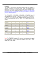
6.3 I/O Expansion Board for A/D, D/A, DI, DO Input Range D/A Output Range Used with I-7188XA/ XB / XC / XG / EX / EG 1 0~2.5V -- -- XC -- 4 0~20Ma -- -- XC -- -- 7 0~20Ma -- -- XB / XG / EX / EG A/D, DI, DO 2 6 2 0~20mA -- -- XB / XG / EX / EG X300 D/A -- -- -- -- 2 0~4.095V XC X301 A/D, D/A -- -- 1 0~2.5V 1 0~4.
Model X507 Description D/I D/O RS-422 4 Channels One channel 4 Speed Used with I-7188XA/ XB / XC / XG / EX / EG 115.2K XB / XG / EX / EG TxD+, TxD-, RxD+, RxDX508 RS-232 4 4 One channel ( 5-wire ) 115.2K XB / XG / EX / EG X509 RS-232 4 4 Two channels ( 3-wire ) 115.2K XB / XG / EX / EG X510 RS-232 5 5 115.2K XB / XG / EX / EG 115.2K XB / XG / EX / EG 115.2K XB / XG / EX / EG 115.
7. X0xx I/O Expansion Boards 7.
7.
7.3 X002 : Prototype Board Size : 115mm * 170mm JP1 J1 Gnd CLOCKA INT0 VCC Gnd TO_0 TI_ 0 SCLK VCC DIO4 U1 2 4 6 8 10 12 14 16 18 20 1 3 5 7 9 11 13 15 17 19 A0 Gnd A1 ARDY A2 INT1 RESET RESET\ VCC TO_ 1 RD\ TI _1 CS\ DIO9 DIO14 VCC C1 0.
7.4 X003: Test Board 1 For I-7188XA (D), I-7188XC (D) & 7521 Power consumption : 0.2W The X003 is self board. It can test DI, DO, System clock, Data Bus, Serial Bus. When you want to test DI and DO of I-7188XC (D) or I-7521, Please connect DI1 to DO1, DI2 to DO2, DI3 to DO3. When you want to test DI and DO of I-7188XA (D) or I-7521, Please connect DI1 to DO1, DI2 to DO2. I/O Expansion Bus for 7188X/7188E User’s Manual, Jun/2004 v1.
7.5 X004: Test Board 2 For I-7188XB (D), I-7188XG (D), I-7188EX (D), I-7188EG (D) Power consumption : 0.2W The X004 is self board. It can test DI, DO, System clock, Data Bus, Serial Bus. When you want to test DI and DO of I-7188XB (D) or I-7188XG (D), Please connect DI1 to DO1. and connect for define pins: 1 to 8, 2 to 9, 3 to 10, 4 to 11, 5 to 12, 6 to 13, 7 to 14. .
Run dido.exe for I-7188EX(D) / I-7188EG(D). i7188e>dido S_CLK --> DIO9 OK!!! DIO4 --> DIO14 OK!!! DIO4 <-- DIO14 OK!!! Data Bus Test OK! Test Timer 0 10 Timer0/INT0 Test OK Test Timer 1 10(00000) Timer1/INT1 Test OK I/O Expansion Bus for 7188X/7188E User’s Manual, Jun/2004 v1.
Run dido.exe for I-7188XB(D) / I-7188XG(D). 7188XB>dido Test DI/DO 1(Please connect DI1 to DO1) Set Do 1 to Low Now DI1 is low -->[ DI ----> OK ]. Set Do1 to High Now DI1 is high -->[ DI ----> OK ]. Set Do1 to Low Now DI1 is low -->[ DI ----> OK ]. S_CLK --> DIO9 OK!!! DIO4 --> DIO14 OK!!! DIO4 <-- DIO14 OK!!! Data Bus Test OK! Test Timer 0 10 Timer0/INT0 Test OK Test Timer 1 10(00000) Timer1/INT1 Test OK I/O Expansion Bus for 7188X/7188E User’s Manual, Jun/2004 v1.
8. X1xx I/O Expansion Boards 8.1 X100: DI * 8 8.1.1 Specifications: For I-7188XC (D) Digital Input : Channels : 8 Input Range / Type : Logic high level (3.5V~30V), Logic low level (0V~1V) Isolated : none. 8.1.2 Pin Assignment: (X100) COM2 Note: refer to section 3. for A/D, D/A, DI, DO wire connection. I/O Expansion Bus for 7188X/7188E User’s Manual, Jun/2004 v1.
8.1.3 Jumper Setting: Note: user should remove R19, R20, R21, R22 and R23 in the 7188XC first. J1: I/O expansion bus, connect to J1 of 7188XC J2: I/O expansion bus, connect to J2 of 7188XC J7: Three channels of 8 DI TP0: Original function on 7188XC TP1: Five channels of 8 DI Jumper: Select TP0 or TP1 function TP0: J9 and J8 closed TP1: J9 and J10 closed 8.1.4 Programming: DiVal = inportb(BASE); /* for all 8-channels */ Note: 1. The default value of BASE is 0. 2.
8.2 X101: DO * 8 8.2.1 Specifications: For I-7188XC (D) Power consumption: 0.4 W Digital Output: Channels: 8 Output: TTL level High Voltage : 2.4V (Min) Low Voltage : 0.8 (Max) Sink current: 64mA (Max) Isolated: none. 8.2.2 Pin Assignment: (X101) COM2 Note: refer to section 3. for A/D, D/A, DI, DO wire connection. I/O Expansion Bus for 7188X/7188E User’s Manual, Jun/2004 v1.
8.2.3 Jumper Setting: Note: user should remove R19, R20, R21, R22 and R23 in the 7188XC first. J1: I/O expansion bus, connect to J1 of 7188XC J2: I/O expansion bus, connect to J2 of 7188XC J7: Three channel of 8 D/O TP0: Original function on 7188XC TP1: Five channel of 8 D/O Jumper: Select TP0 or TP1 function TP0: JP9 and JP8 closed TP1: JP9 and JP10 closed 8.2.4 Programming: outportb(BASE, DoVal); /* for all 8-channels */ Note: 1. The default value of BASE is 0. 2.
8.3 X10²: Relay * 2 8.3.1 Specifications : For I-7188XC (D) Relay Output : • • • • • • • • Channels : 2 (Form "C") Max. Switching voltage : 220Vdc, 250Vac Max. Switching current : 2A Max. Carrying current : 2A Surge Strength : 1,500V Electrical endurance : Typical 500,000 operation at 30Vdc / 1A Typical 100,000 operation at 125Vac / 0.5A Relay on time (typical) : 6ms Relay off time (typical) : 6ms 8.3.2 Pin Assignment: (X102) COM2 NO ( Normal Open ) O.C.
8.3.3 Jumper Setting: Note: user should remove R19, R20, R21, R22 and R23 in the 7188XC first. J1: I/O expansion bus, connect to J1 of 7188XC J2: I/O expansion bus, connect to J2 of 7188XC J7: One channel of relay output TP0: Original function on 7188XC TP1: One channel of relay output Jumper: Select TP0 or TP1 function TP0: JP9 and JP8 closed TP1: JP9 and JP10 closed 8.3.
8.4 X10³: Isolated DI * 7 8.4.1 Specifications: For I-7188XC (D) Power consumption: 0.3 W Digital Input : Channels : 7 Input Range / Type : Logic high level (3.5V~30V), Logic low level (0V~1V) Isolated digital input. 8.4.2 Pin Assignment: (X103) COM2 Note: refer to section 3. for A/D, D/A, DI, DO wire connection. I/O Expansion Bus for 7188X/7188E User’s Manual, Jun/2004 v1.
8.4.3 Jumper Setting: Note: user should remove R19, R20, R21, R22, R23 in the 7188XC first. J1: I/O expansion bus, connect to J1 of 7188XC J2: I/O expansion bus, connect to J2 of 7188XC J7: Two channels of isolated DI TP0: Original function on 7188XC TP1: Five channels of isolated DI Jumper: Select TP0 or TP1 function TP0: JP9 and JP8 closed TP1: JP9 and JP10 closed 8.4.
8.5 X10⁴: D/I/O * 8, single-bit 8.5.1 Specifications: For I-7188XC (D) Power consumption: 0.3 W Digital Input / Output: Channels: 8 Input / Output: each channel can be programmed to D/I or D/O. Input Range: 0~5V(Max) Isolated: none. 8.5.2 Pin Assignment: (X104) COM2 Note: Provide functions of DI and DO from CPU. I/O Expansion Bus for 7188X/7188E User’s Manual, Jun/2004 v1.
8.5.3 Jumper Setting: Note: user should remove R19, R20, R21, R22 and R23 in the 7188XC first. J1: I/O expansion bus, connect to J1 of 7188XC J2: I/O expansion bus, connect to J2 of 7188XC J7: Three channels of 8 D/I/O TP0: Original function on 7188XC TP1: Five channels of 8 D/I/O Jumper: Select TP0 or TP1 function TP0: JP9 and JP8 closed TP1: JP9 and JP10 closed 8.5.
void SetTi1Dir(int dir); void SetTi1High(void); void SetTi1Low(void); int GetTi1(void); void SetTo1Dir(int dir); void SetTo1High(void); void SetTo1Low(void); int GetTo1(void); void SetTi0Dir(int dir); void SetTi0High(void); void SetTi0Low(void); int GetTi0(void); void SetTo0Dir(int dir); void SetTo0High(void); void SetTo0Low(void); int GetTo0(void); void SetDo1High(void); void SetDo1Low(void); int GetDo1(void); void SetDo2High(void); void SetDo2Low(void); int GetDo2(void); void SetDo3High(void); void SetDo3
8.6 X10⁵: D/I/O * 8, 8-bit 8.6.1 Specifications: For I-7188XC Power consumption: 0.3 W Digital Input: Channels: 8 Input Range / Type: Logic high level (3.5V~30V), Logic low level (0V~1V) Isolated: none Digital Output: Channels: 8 Output: TTL level Isolated: none 8.6.2 Pin Assignment: (X105) COM2 Note: refer to section 3. for A/D, D/A, DI, DO wire connection. I/O Expansion Bus for 7188X/7188E User’s Manual, Jun/2004 v1.
8.6.3 Jumper Setting: Note: user should remove R19, R20, R21, R22 and R23 in the 7188XC first. J1: I/O expansion bus, connect to J1 of 7188XC J2: I/O expansion bus, connect to J2 of 7188XC J7: Three channels of 8 D/I/O TP0: Original function on 7188XC TP1: Five channels of 8 D/I/O Jumper: Select TP0 or TP1 function TP0: JP9 and JP8 closed TP1: JP9 and JP10 closed 8.6.4 Programming DiVal = inportb(BASE); /* for all 8-channels */ Note: 1. The default value of BASE is 0. 2.
If DIO14 is HIGH select D/I*8 D/I signals are come from J5 Select D/I*8 as following: SetDio14Dir(0); /* select DIO14 as D/O SetDio14High(); /* select D/I*8 DiVal=inportb(BASE); /* read D/I*8 (from J5) Select D/I*8 as following: SetDio14Dir(0); /* select DIO14 as D/O SetDio14Low(); /* select D/O*8 outportb(BASE,DoVal); /* set value of D/O*8 (to J5) DiVal=inportb(BASE); /* D/O*8 read back */ */ */ */ */ */ */ I/O Expansion Bus for 7188X/7188E User’s Manual, Jun/2004 v1.
8.7 X10⁶: DO *2 or DI *3 8.7.1 Specifications: For I-7188XC Digital Input: Channels: 3 Input Range / Type: Logic high level (3.5V~30V), Logic low level (0V~1V) Isolated: none Digital Output: Channels:3 Open-collector Output: 250 mA / 30V max Isolated: none 8.7.2 Pin Assignment: (X106) COM2 Note: refer to section 3. for A/D, D/A, DI, DO wire connection. I/O Expansion Bus for 7188X/7188E User’s Manual, Jun/2004 v1.
8.7.3 Jumper Setting: J1: I/O expansion bus, connect to J1 of 7188XC J2: I/O expansion bus, connect to J2 of 7188XC J7: Three channels of D/I or two channels of D/O Jumper: Select D/I or D/O function D/I: j4, j5,j6 select 2-3 (default setting) D/O: j4, j5, j6 select 1-2 8.7.
8.8 X10⁷: DI * 6 and DO * 7 8.8.1 Specifications: For I-7188XB, I-7188XG, I-7188EX, I-7188EG Digital Input : Channels: 6 Input Range / Type: Logic high level (3.5V~30V), Logic low level (0V~1V) Isolated: none Digital Output: Channels: 7 Open-collector Output: 100 mA / 30V max Isolated: none 8.8.2 Pin Assignment : (X107) Note: refer to section 3. for A/D, D/A, DI, DO wire connection. I/O Expansion Bus for 7188X/7188E User’s Manual, Jun/2004 v1.
8.8.3 Programming : DiVal = inportb(BASE); Note: /* for all 6 channels */ 1. The default value of BASE is 1. 2. It is not recommended to change the value of BASE from 0 to another value. 3. DiVal=0x00 DiVal=0x01 DiVal=0x3F outportb(BASE, DoVal); Note: all 6-channel are Low Chennel_0 is High, the other channels are Low all 6-channel are High /* for all 7 channels */ 1. The default value of BASE is 0. 2. It is not recommended to change the value of BASE from 0 to another value. 3.
8.9 X10⁸: PWM * 2 8.9.1 Specifications: For I-7188XC Power consumption: 0.5 W Frequency : Low frequency : 40Hz High frequency : 100KHz Open-collector output: 250mA/30V, Max (Per channel) 8.9.2 Pin Assignment: (X108) COM2 I/O Expansion Bus for 7188X/7188E User’s Manual, Jun/2004 v1.
8.9.3 Programming : Note: How to download PWM.exe, Refer to Section 1.5 1. Download : COM1 will download PWM.exe & AUTOEXEC.bat So $aaB0115200 --> change COM1 to 115200 So $aaB09600 --> change COM1 to 9600 2. default setting: address=01, baud rate=9600 3. Command Sets : Press Alt + L [Enter] under MinOS7. Example of how frequency is used.
#01B00 --> !01 CHAN_0 Off #01C0 --> !01 100 1 1 0 5. Run Visual Basic: I/O Expansion Bus for 7188X/7188E User’s Manual, Jun/2004 v1.
8.10 X10⁹: PhotoMOS Relay * 7 8.10.1 Specifications: For I-7188XB, I-7188XG, I-7188EX, I-7188EG Channels: 7 (Form A) Continuous load current:120mA (peak AC) Peak load current: 0.3A Output Off state leakage current : 1Ua Output On resistance : 25Ohm Load voltage : 350V(peak AC) Turn On time : 0.23ms (Typical) Turn Off time : 0.04ms (Typical) Input / Output Isolation : 1,500V AC 8.10.2 Pin Assignment : (X109) 8.10.3 Programming : outportb(BASE, DoVal); Note: /* for all 7-channels */ 1.
8.11 X110: 14 Channels D/I 8.11.1 Specifications: For I-7188XB, I-7188XG, I-7188EX, I-7188EG Digital Input : Channels: 14 Input Range / Type: Logic high level (3.5V~30V), Logic low level (0V~1V) Isolated: none 8.11.2 Pin Assignment : (X110) Note: refer to section 3. for A/D, D/A, DI, DO wire connection. 8.11.
8.12 X111: 13 Channels D/O 8.12.1 Specifications: For I-7188XB, I-7188XG, I-7188EX, I-7188EG Digital Output: Channels: 13 Open-collector Output: 100 mA / 30V max Isolated: none 8.12.2 Pin Assignment : (X111) Note: refer to section 3. for A/D, D/A, DI, DO wire connection. 8.12.3 Programming : outpw(port, DoVal); /* for all 13-channels */ Please notice that Base address “0x0080” not used.
9. X2xx I/O Expansion Boards 9.1 X200: AD*1 9.1.1 Specifications : For I-7188XC Analog Input: Channel : 1 ( Single-Ended ) Resolution : 12bit Input Range/Type : 0 ~ 2.5 V Sampling rate : 900 Hz Isolated : none 9.1.2 Pin Assignment : (X200) COM2 Note: refer to section 3. for A/D, D/A, DI, DO wire connection. 9.1.3 Programming : For Software Installation & Demo Program, Refer to Section 2.2.2 I/O Expansion Bus for 7188X/7188E User’s Manual, Jun/2004 v1.
9.2 X201: AD*1 9.2.1 Specifications : For I-7188XC Power consumption: 0.4W Analog Input: Channel : 1 ( Differential ) Resolution : 12bit Input Range/Type : 0 ~ 20mA Sampling rate : 900 Hz Isolated : none 9.2.2 Pin Assignment : (X201) COM2 Note: refer to section 3. for A/D, D/A, DI, DO wire connection. I/O Expansion Bus for 7188X/7188E User’s Manual, Jun/2004 v1.
9.2.3 Jumper Setting: Note: user should remove R19, R20, R21, R22, R23 in the 7188XC first. J7: I1+, I1-, I2+ TP0, TP1: I2-, I3+, I3- ,I4+, I4TP0: Original function on 7188XC TP1: Five channels of isolated DI Jumper: Select TP0 or TP1 function TP0: JP9 and JP8 closed TP1: JP9 and JP10 closed 9.2.4 Programming : For Software Installation & Demo Program, Refer to Section 2.2.2 I/O Expansion Bus for 7188X/7188E User’s Manual, Jun/2004 v1.
9.3 X202: AD*7 9.3.1 Specifications : For I-7188XB, I-7188XG, I-7188EX, I-7188EG Power consumption: 0.7W Analog Input: Channel : 7 ( Differential ) Resolution : 12bit Input Range/Type : 0 ~ 20mA Sampling rate : 1800 Hz Isolated : none 9.3.2 Pin Assignment : (X202) Note: refer to section 3. for A/D, D/A, DI, DO wire connection. 9.3.3 Programming : For Software Installation & Demo Program, Refer to Section 2.2.2 I/O Expansion Bus for 7188X/7188E User’s Manual, Jun/2004 v1.
9.4 X203: AD*2 + DO*6 + DI*2 9.4.1 Specifications : For I-7188XB, I-7188XG, I-7188EX, I-7188EG Power consumption: 0.7W Analog Input: Channel : 2 ( Differential ) Resolution : 12bit Input Range/Type : 0 ~ 20mA Sampling rate : 1800 Hz Digital Input : Channels: 2 Input Range / Type: Logic high level (3.5V~30V), Logic low level (0V~1V) Isolated: none Digital Output: Channels: 6 Open-collector Output: 100 mA / 30V max Isolated: none 9.4.2 Pin Assignment : (X203) Note: Refer to section 3.
10. X3xx I/O Expansion Boards 10.1 X300: DA * 2 10.1.1 Specifications : For I-7188XC Analog Output: Channel : 2 Resolution : 12bit Input Range/Type : 0 ~ 4.095V Sampling rate : 650 Hz Isolated : none 10.1.2 Pin Assignment : (X300) COM2 Note: refer to section 3. for A/D, D/A, DI, DO wire connection. 10.1.3 Programming : For Software Installation & Demo Program, Refer to Section 2.2.2 I/O Expansion Bus for 7188X/7188E User’s Manual, Jun/2004 v1.
10.2 X301: DA * 1 + AD * 1 10.2.1 Specifications : For I-7188XC Analog Output: Channel : 1 Resolution : 12bit Input Range/Type : 0 ~ 4.095V Sampling rate : 650 Hz Isolated : none Analog Intput: Channel : 1 ( Single-Ended ) Resolution : 12bit Input Range/Type : 0 ~ 2.5V Sampling rate : 900 Hz Isolated : none 10.2.2 Pin Assignment : (X301) COM2 Note: refer to section 3. for A/D, D/A, DI, DO wire connection. I/O Expansion Bus for 7188X/7188E User’s Manual, Jun/2004 v1.
10.2.3 Programming : void AnalogOutput(int DataIn ) DataIn = 0 – 4095 (Note 4095 int AnalogIn( void ) Return value= 0 - 4095 Mapping formula: Vref / 4096 (Note: Vref=2.5v) 4.095V) For Software Installation & Demo Program, Refer to Section 2.2.2 I/O Expansion Bus for 7188X/7188E User’s Manual, Jun/2004 v1.
10.3 X302: DA * 1 + AD * 1 10.3.1 Specifications : For I-7188XC Analog Output: Channel : 1 Resolution : 12bit Input Range/Type : +/- 5V Sampling rate : 650 Hz Isolated : none Analog Intput: Channel : 1 ( Single-Ended ) Resolution : 12bit Input Range/Type : +/- 5V Sampling rate : 900 Hz Isolated : none 10.3.2 Pin Assignment : (X302) COM2 Note: refer to section 3. for A/D, D/A, DI, DO wire connection. I/O Expansion Bus for 7188X/7188E User’s Manual, Jun/2004 v1.
10.3.3 Programming : void AnalogOutput(int DataIn ) DataIn = 0 – 4095 (Note 4095 int AnalogIn( void ) Return value= 0 - 4095 Mapping formula: Vref / 4096 (Note: Vref=5v) 4.095V) For Software Installation & Demo Program, Refer to Section 2.2.2 [Software specific] Input/Output range: Decimal integer: Hexadecimal: [A/D] sampling rate: Accuracy==> [D/A] thoughput : Accuracy==> -5.0V -0.0V +0.0V 0 000 2047 7FF 2048 800 +5.
10.4 X303: AD*1 + DA*1 + DO*6 + DI*4 10.4.1 Specifications : For I-7188XB, I-7188XG, I-7188EX, I-7188EG Analog Output: Channel : 1 Resolution : 12bit Input Range/Type : +/- 5V Sampling rate : 1300 Hz Isolated : none Analog Intput: Channel : 1 ( Single-Ended ) Resolution : 12bit Input Range/Type : +/- 5V Sampling rate : 1800 Hz Isolated : none Digital Input : Channels: 4 Input Range / Type: Logic high level (3.
10.4.2 Pin Assignment : (X303) Note: Refer to section 3. for A/D, D/A, DI, DO wire connection. 10.4.3 Programming : For Software Installation & Demo Program, Refer to Section 2.2.2 [Software specific] Input/Output range: Decimal integer: Hexadecimal: [A/D] sampling rate: Accuracy==> [D/A] thoughput : Accuracy==> [D/O] throughput: -5.0V 0 000 -0.0V 2047 7FF +0.0V 2048 800 +5.0V 4095 FFF 1800 data/sec (with floating convertion) Typical: +/- 1 LSB (+- 2.4 mV) Maximum: +/- 2 LSB (+- 4.
10.5 X304: AD*3 + DA*1 + DO*4 + DI*4 10.5.1 Specifications : For I-7188XB, I-7188XG, I-7188EX, I-7188EG Analog Output: Channel : 1 Resolution : 12bit Input Range/Type : +/- 5V Sampling rate : 1300 Hz Isolated : none Analog Intput: Channel : 3 ( Single-Ended ) Resolution : 12bit Input Range/Type : +/- 5V Sampling rate : 1800 Hz Isolated : none Digital Input : Channels: 4 Input Range / Type: Logic high level (3.
10.5.2 Pin Assignment : (X304) Note: Refer to section 3. for A/D, D/A, DI, DO wire connection. 10.5.3 Programming : For Software Installation & Demo Program, Refer to Section 2.2.2 [Software specific] Input/Output range: Decimal integer: Hexadecimal: [A/D] sampling rate: Accuracy==> [D/A] thoughput : Accuracy==> [D/O] throughput: -5.0V 0 000 -0.0V 2047 7FF +0.0V 2048 800 +5.0V 4095 FFF 1800 data/sec (with floating convertion) Typical: +/- 1 LSB (+- 2.4 mV) Maximum: +/- 2 LSB (+- 4.
10.6 X305: AD*7 + DA*1 + DO*2 + DI*2 10.6.1 Specifications : For I-7188XB, I-7188XG, I-7188EX, I-7188EG Analog Output: Channel : 1 Resolution : 12bit Input Range/Type : +/- 5V Sampling rate : 1300 Hz Isolated : none Analog Intput: Channel : 7 ( Single-Ended ) Resolution : 12bit Input Range/Type : +/- 5V Sampling rate : 1800 Hz Isolated : none Digital Input : Channels: 2 Input Range / Type: Logic high level (3.
10.6.2 Pin Assignment : (X305) Note: Refer to section 3. for A/D, D/A, DI, DO wire connection. 10.6.3 Programming : For Software Installation & Demo Program, Refer to Section 2.2.2 [Software specific] Input/Output range: Decimal integer: Hexadecimal: [A/D] sampling rate: Accuracy==> [D/A] thoughput : Accuracy==> [D/O] throughput: -5.0V 0 000 -0.0V 2047 7FF +0.0V 2048 800 +5.0V 4095 FFF 1800 data/sec (with floating convertion) Typical: +/- 1 LSB (+- 2.4 mV) Maximum: +/- 2 LSB (+- 4.
10.7 X306: AD*2 10.7.1 Specifications : For I-7188XC Power consumption: 0.4W Analog Input: Channel : 2 ( Single-Ended ) Resolution : 12bit Input Range/Type : + / - 10 V Sampling rate : 900 Hz Isolated : none 10.7.2 Pin Assignment : (X306) COM2 Note: refer to section 3. for A/D, D/A, DI, DO wire connection. 10.7.3 Programming : For Software Installation & Demo Program, Refer to Section 2.2.2 I/O Expansion Bus for 7188X/7188E User’s Manual, Jun/2004 v1.
10.8 X307: AD*8 10.8.1 Specifications : For I-7188XB, I-7188XG, I-7188EX, I-7188EG Power consumption: 0.7W Analog Input: Channel :8 ( Single-Ended ) Resolution : 12bit Input Range/Type : + / - 10V Sampling rate : 1800 Hz Isolated : none 10.8.2 Pin Assignment : (X307) Note: refer to section 3. for A/D, D/A, DI, DO wire connection. 10.8.3 Programming : For Software Installation & Demo Program, Refer to Section 2.2.2 I/O Expansion Bus for 7188X/7188E User’s Manual, Jun/2004 v1.
10.9 X308: AD*4 + DO*6 10.9.1 Specifications : For I-7188XB, I-7188XG, I-7188EX, I-7188EG Analog Intput: Channel : 4 ( Single-Ended ) Resolution : 12bit Input Range/Type : 0 ~ 10V Sampling rate : 1800 Hz Isolated : none Digital Output: Channels: 6 Open-collector Output: 100 mA / 30V max Isolated: none 10.9.2 Pin Assignment : (X308) Note: Refer to section 3. for A/D, D/A, DI, DO wire connection. I/O Expansion Bus for 7188X/7188E User’s Manual, Jun/2004 v1.
10.9.3 Programming : For Software Installation & Demo Program, Refer to Section 2.2.2 [Software specific] Input/Output range: Decimal integer: Hexadecimal: [A/D] sampling rate: Accuracy==> [D/O] throughput: 0V 0 000 4.9V 2047 7FF 5V 2048 800 10V 4095 FFF 1800 data/sec (with floating convertion) Typical: +/- 1 LSB (+- 2.4 mV) Maximum: +/- 2 LSB (+- 4.8 mV) can generates 2KHz square wave signals. I/O Expansion Bus for 7188X/7188E User’s Manual, Jun/2004 v1.
10.10 10.10.1 X310: AD*2 + DA*2 + DO*3 + DI*3 Specifications : For I-7188XB, I-7188XG, I-7188EX, I-7188EG Analog Output: Channel : 2 Resolution : 12bit Input Range/Type : 0 ~ 10V Sampling rate : 1300 Hz Isolated : none Analog Intput: Channel : 2 ( Differential ) Resolution : 12bit Input Range/Type : Ch0 : 0 ~ 20 mA Ch1 : 0 ~ 10 V Sampling rate : 1800 Hz Isolated : none Digital Input : Channels: 3 Input Range / Type: Logic high level (3.
10.10.2 Pin Assignment : (X310) Note: Refer to section 3. for A/D, D/A, DI, DO wire connection. 10.10.3 Programming : For Software Installation & Demo Program, Refer to Section 2.2.2 [Software specific] Input/Output range: Decimal integer: Hexadecimal: [A/D] sampling rate: Accuracy==> [D/A] thoughput : Accuracy==> [D/O] throughput: 0V 0 000 4.9V 2047 7FF 5.0V 2048 800 10V 4095 FFF 1800 data/sec (with floating convertion) Typical: +/- 1 LSB (+- 2.4 mV) Maximum: +/- 2 LSB (+- 4.
11. X4xx I/O Expansion Boards 11.1 X400:Timer/counter *3 11.1.1 Specifications : For I-7188XC Analog Input: Channel : 3 16 bit timer/counter Isolated : none 11.1.2 Pin Assignment & Jumper Setting : (X400) COM2 Note: You can used 3 channels 16-bit counters or 1 channel 16-bit and 1 channel 32-bit J7: TP0: TP1: for counter-0 Original function on 7188XC for counter1, counter2 I/O Expansion Bus for 7188X/7188E User’s Manual, Jun/2004 v1.
Jumper setting for 8254: 1-2 ON 2-3 ON CLK0 T1 CLK0=TO_0 T1 CLK0=pin1 of J5 G0 T2 G0=always High T2 G0=pin2 of J5 OUT0 OUT0 to INT0 & pin3 of J5 CLK1 T4 T4 CLK0=pin4 of J5 G1 Always High OUT1 OUT1 to T3.1 & T5.1 & T6.1 CLK2 T3 T3 CLK2=pin5 of J5 G2 Always High OUT2 OUT2 to T5.3 & T7.1 CLK1=TO_1 CLK2=OUT1 T1 is used to select internal TO_0 or external signal for CLK0 T2 is used to select High or external signal for G0 T3 is used to control 16-bit/32-bit counter.
This page is blank… I/O Expansion Bus for 7188X/7188E User’s Manual, Jun/2004 v1.
This page is blank… I/O Expansion Bus for 7188X/7188E User’s Manual, Jun/2004 v1.
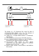
12. X5xx I/O Expansion Boards 12.1 X500: RS232 * 1 12.1.1 Specifications For I-7188XC Parallel I/O : RS-232 port : 1 COM3 : TXD, RXD, RTS, CTS, DSR, DTR, DCD, RI, GND 16550 compatible Internal FIFO : 16 bytes Transmission speed: 115.2K BPS max. Modem control Isolated : none 12.1.2 Pin Assignment & Jumper Setting (X500) COM2 Figure 1 Note: There are two type of functions in X500. 1. COM3 : TXD, RXD, RTS, CTS, DSR, DTR, DCD, RI, GND This function without case. 2.
J1 TP0 TP1 J5 J7 J3 7188XC X500 J2 J1: J2: J7: J3: I/O expansion bus, connect to J1 of 7188XC I/O expansion bus, connect to J2 of 7188XC Three wires of RS-232 (RXD, TXD, GND) Pin Assignment : refer to Figure 1 on page 90. 9-pin connector of RS-232, connect to modem Block Diagram 7188XC/7188XB X500 J1 J1 9-pin RS-232 I/O Expansion Modem Bus J2 J2 J3 3-pin RS-232 J7 J7 I/O Expansion Bus for 7188X/7188E User’s Manual, Jun/2004 v1.
12.1.3 Programming : Compatible to COM3 of 7188X software library int InstallCom3(unsigned long baud, int data, int parity, int stop); int RestoreCom3(void); int IsCom3(void); int ToCom3(int data); int ToCom3Str(char *str); int ToCom3Bufn(char *buf,int no); int printCom3(char *fmt,...
12.2 X501: RS232 * 1 12.2.1 Specifications For I-7188XC Parallel I/O : RS-232 port : 1 COM3 : TXD, RXD, RTS, CTS, GND 16550 compatible Internal FIFO : 16 bytes Transmission speed: 115.2K BPS max. Isolated : none 12.2.2 Pin Assignment : (X501) 12.2.3 COM2 Programming : For Software Installation & Demo Program, Refer to Section 2.2.2 I/O Expansion Bus for 7188X/7188E User’s Manual, Jun/2004 v1.
12.3 X502: RS232 * 1 12.3.1 Specifications For I-7188XC Parallel I/O : RS-232 port : 2 COM3 : TXD, RXD, RTS, CTS, GND COM4: TXD, RXD, GND 16550 compatible Internal FIFO : 16 bytes Transmission speed: 115.2K BPS max. Isolated : none 12.3.2 Pin Assignment : (X502) 12.3.3 COM2 Programming : For Software Installation & Demo Program, Refer to Section 2.2.2 I/O Expansion Bus for 7188X/7188E User’s Manual, Jun/2004 v1.
12.4 X503: RS232 * 1 12.4.1 Specifications : For I-7188XB, I-7188XG, I-7188EX, I-7188EG Parallel I/O : RS-232 port : 1 COM3 : TXD, RXD, RTS, CTS, GND 16550 compatible Internal FIFO : 16 bytes Transmission speed: 115.2K BPS max. Isolated : none 12.4.2 Pin Assignment : (X503) 12.4.3 Programming : I-7188E4 and X503 + I-7188EX are software the same. I-7523 and X503 + I-7188XB are software the same. For Software Installation & Demo Program, Refer to Section 2.2.
12.5 X504: RS232 * 2 12.5.1 Specifications : For I-7188XB, I-7188XG, I-7188EX, I-7188EG Parallel I/O : COM3 : TXD, RXD, RTS, CTS, GND COM4 : TXD, RXD, RTS, CTS, DSR, DTR, DCD, RI, GND 16550 compatible Internal FIFO : 16 bytes Transmission speed: 115.2K BPS max. Modem control Isolated : none 12.5.2 Pin Assignment : (X504) 12.5.3 Programming : I-7188E4 and X504 + I-7188EX are software the same. For Software Installation & Demo Program, Refer to Section 2.2.
12.6 X505: RS232 * 3 12.6.1 Specifications : For I-7188XB, I-7188XG, I-7188EX, I-7188EG Parallel I/O : COM3 : TXD, RXD, RTS, CTS, GND COM4 : TXD, RXD, RTS, CTS, GND COM5 : TXD, RXD, RTS, CTS, GND 16550 compatible Internal FIFO : 16 bytes Transmission speed: 115.2K BPS max. Isolated : none 12.6.2 Pin Assignment : (X505) 12.6.3 Programming : I-7188E5 and X505 + I-7188EX are software the same. I-7524 and X505 + I-7188XB are software the same.
12.7 X506: RS232 * 6 12.7.1 Specifications : For I-7188XB, I-7188XG, I-7188EX, I-7188EG Parallel I/O : COM3 : TXD, RXD, GND COM4 : TXD, RXD, GND COM5 : TXD, RXD, GND COM6 : TXD, RXD, GND COM7 : TXD, RXD, GND COM8: TXD, RXD, GND 16550 compatible Internal FIFO : 16 bytes Transmission speed: 115.2K BPS max. Isolated : none 12.7.2 Pin Assignment : (X506) 12.7.3 Programming : I-7188E8 and X506 + I-7188EX are software the same. I-7527 and X506 + I-7188XB are software the same.
12.8 X507: RS422 * 1 + DO*4 + DI*4 12.8.1 Specifications : For I-7188XB, I-7188XG, I-7188EX, I-7188EG Parallel I/O : COM3 : TxD+, TxD -RxD+, RxD 16550 compatible Internal FIFO : 16 bytes Transmission speed: 115.2K BPS max. Isolated : none Digital Input : Channels: 4 Input Range / Type: Logic high level (3.5V~30V), Logic low level (0V~1V) Isolated: none Digital Output: Channels: 4 Open-collector Output: 100 mA / 30V max Isolated: none I/O Expansion Bus for 7188X/7188E User’s Manual, Jun/2004 v1.
12.8.2 Pin Assignment : (X507) Note: refer to section 3. for A/D, D/A, DI, DO wire connection. 12.8.3 Programming : I-7188E3 and X507 + I-7188EX are software the same. I-7522A and X507 + I-7188XB are software the same. For Software Installation & Demo Program, Refer to Section 2.2.2 I/O Expansion Bus for 7188X/7188E User’s Manual, Jun/2004 v1.
12.9 X508: RS232 * 1 + DO*4 + DI*4 12.9.1 Specifications : For I-7188XB, I-7188XG, I-7188EX, I-7188EG Parallel I/O : COM3 : TXD, RXD, RTS, CTS, GND 16550 compatible Internal FIFO : 16 bytes Transmission speed: 115.2K BPS max. Isolated : none Digital Input : Channels: 4 Input Range / Type: Logic high level (3.5V~30V), Logic low level (0V~1V) Isolated: none Digital Output: Channels: 4 Open-collector Output: 100 mA / 30V max Isolated: none I/O Expansion Bus for 7188X/7188E User’s Manual, Jun/2004 v1.
12.9.2 Pin Assignment : (X508) Note: refer to section 3. for A/D, D/A, DI, DO wire connection. 12.9.3 Programming : I-7188E3-232 and X508 + I-7188EX are software the same. I-7522A and X508 + I-7188XB are software the same. For Software Installation & Demo Program, Refer to Section 2.2.2 I/O Expansion Bus for 7188X/7188E User’s Manual, Jun/2004 v1.
12.10 12.10.1 X509: RS232 * 2 + DO*4 + DI*4 Specifications : For I-7188XB, I-7188XG, I-7188EX, I-7188EG Parallel I/O : COM3 : TXD, RXD, GND COM4 : TXD, RXD, GND 16550 compatible Internal FIFO : 16 bytes Transmission speed: 115.2K BPS max. Isolated : none Digital Input : Channels: 4 Input Range / Type: Logic high level (3.
12.10.2 Pin Assignment : (X509) Note: refer to section 3. for A/D, D/A, DI, DO wire connection. 12.10.3 Programming : For Software Installation & Demo Program, Refer to Section 2.2.2 I/O Expansion Bus for 7188X/7188E User’s Manual, Jun/2004 v1.
12.11 12.11.1 X510: RS232 * 1 + DO*5 + DI*5 Specifications : For I-7188XB, I-7188XG, I-7188EX, I-7188EG EEPROM: 128K * 2 bytes For X510 EEPROM: 128K * 1 bytes For X510-128 Parallel I/O : COM3 : TXD, RXD, GND 16550 compatible Internal FIFO : 16 bytes Transmission speed: 115.2K BPS max. Isolated : none Digital Input : Channels: 5 Input Range / Type: Logic high level (3.
12.11.2 Pin Assignment : (X510) Note: refer to section 3. for A/D, D/A, DI, DO wire connection. 12.11.3 Programming : I-7188E3 and X510 + I-7188EX are software the same. For Software Installation & Demo Program, Refer to Section 2.2.2 I/O Expansion Bus for 7188X/7188E User’s Manual, Jun/2004 v1.
12.12 X511: RS485 * 3 12.12.1 Specifications : For I-7188XB, I-7188XG, I-7188EX, I-7188EG Parallel I/O : COM3 : Data+, DataCOM4 : Data+, DataCOM5 : Data+, Data16550 compatible Internal FIFO : 16 bytes Transmission speed: 115.2K BPS max. Isolated : none 12.12.2 Pin Assignment : (X511) 12.12.3 Programming : I-7188E5 and X511 + I-7188EX are software the same. I-7524 and X511 + I-7188XB are software the same. For Software Installation & Demo Program, Refer to Section 2.2.
12.13 12.13.1 X512: RS-232 * 4 + RS485 * 1 Specifications : For I-7188XB, I-7188XG, I-7188EX, I-7188EG Parallel I/O : COM3 : TXD, RXD, GND COM4 : TXD, RXD, GND COM5 : TXD, RXD, GND COM6 : TXD, RXD, GND COM7 : Data+, Data16550 compatible Internal FIFO : 16 bytes Transmission speed: 115.2K BPS max. Isolated : none 12.13.2 Pin Assignment : (X512) 12.13.3 Programming : I-7188E8 and X512 + I-7188EX are software the same. I-7527 and X512 + I7188XB are software the same.
12.14 12.14.1 X560: RS-232 * 3 + 8 M Flash Specifications : ** The module without case. ** For I-7188XA, I-7188XC, I-7188XB, I-7188XG, I-7188EX, I-7188EG Parallel I/O : COM4 : TXD, RXD, GND COM5 : TXD, RXD, GND COM6 : TXD, RXD, GND 16550 compatible Internal FIFO : 16 bytes Transmission speed: 115.2K BPS max. Isolated : none Storage flash, 8M bytes : Endurance : 1,000,000 Program/Erase Cycles Data Retention : 10 years I/O Expansion Bus for 7188X/7188E User’s Manual, Jun/2004 v1.
12.14.2 Pin Assignment : X560 COM1 12.14.3 COM2 Programming : For Software Installation & Demo Program, Refer to Section 2.2.2 I/O Expansion Bus for 7188X/7188E User’s Manual, Jun/2004 v1.
13. X6xx I/O Expansion Boards 13.1 X600 and X601 : Flash ROM 13.1.1 Specifications For I-7188XA, I-7188XC, I-7188XB, I-7188XG, I-7188EX, I-7188EG Power consumption: 0.5W X600: storage flash, 4M bytes Endurance : 1,000,000 Program/Erase Cycles Data Retention : 10 years X601: storage flash, 8M bytes Endurance : 1,000,000 Program/Erase Cycles Data Retention : 10 years 13.1.
13.2 13.2.1 X607 and X608: SRAM Specifications X607 : 128K bytes battery backup X608 : 512K bytes battery backup For I-7188XA, I-7188XC, I-7188XB, I-7188XG, I-7188EX, I-7188EG *** X607 and X608 are support file system. *** Power consumption: 0.5W Introduction: There are two modes of power supplies to SRAM, I-7188(VCC) mode and battery mode. The voltage of the battery is 3 V, the voltage of I- I7188 mode is 5 V. I-7188 (VCC) is the primary power supply when it is powered on.