
Data Sheet
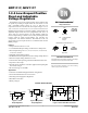


NCP1117, NCV1117
http://onsemi.com
4
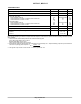
ELECTRICAL CHARACTERISTICS (C
in
= 10 mF, C
out
= 10 mF, for typical value T
A
= 25°C, for min and max values T
A
is the
operating ambient temperature range that applies unless otherwise noted. (Note 6)
Characteristic
Symbol Min Typ Max Unit
Dropout Voltage (Measured at V
out
− 100 mV)
(I
out
= 100 mA)
(I
out
= 500 mA)
(I
out
= 800 mA)
V
in
−V
out
−
−
−
0.95
1.01
1.07
1.10
1.15
1.20
V
Output Current Limit (V
in
−V
out
= 5.0 V, T
A
= 25°C, Note 7) I
out
1000 1500 2200 mA
Minimum Required Load Current for Regulation, Adjustable Output Devices
(V
in
= 15 V)
I
L(min)
− 0.8 5.0 mA
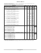
Quiescent Current
1.5 V (V
in
= 11.5 V)
1.8 V (V
in
= 11.8 V)
1.9 V (V
in
= 11.9 V)
2.0 V (V
in
= 12 V)
2.5 V (V
in
= 10 V)
2.85 V (V
in
= 10 V)
3.3 V (V
in
= 15 V)
5.0 V (V
in
= 15 V)
12 V (V
in
= 20 V)
I
Q
−
−
−
−
−
−
−
−
−
3.6
4.2
4.3
4.5
5.2
5.5
6.0
6.0
6.0
10
10
10
10
10
10
10
10
10
mA
Thermal Regulation (T
A
= 25°C, 30 ms Pulse) − 0.01 0.1 %/W
Ripple Rejection (V
in
−V
out
= 6.4 V, I
out
= 500 mA, 10 V
pp
120 Hz Sinewave)
Adjustable
1.5 V
1.8 V
1.9 V
2.0 V
2.5 V
2.85 V
3.3 V
5.0 V
12 V
RR
67
66
66
66
64
62
62
60
57
50
73
72
70
72
70
68
68
64
61
54
−
−
−
−
−
−
−
−
−
−
dB
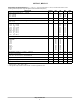
Adjustment Pin Current (V
in
= 11.25 V, I
out
= 800 mA) I
adj
− 52 120
mA
Adjust Pin Current Change
(V
in
−V
out
= 1.4 V to 10 V, I
out
= 10 mA to 800 mA)
DI
adj
− 0.4 5.0
mA
Temperature Stability S
T
− 0.5 − %
Long Term Stability (T
A
= 25°C, 1000 Hrs End Point Measurement) S
t
− 0.3 − %
RMS Output Noise (f = 10 Hz to 10 kHz) N − 0.003 − %V
out
6. NCP1117: T
low
= 0°C , T
high
= 125°C
NCV1117: T
low
= −40°C, T
high
= 125°C
7. The regulator output current must not exceed 1.0 A with V
in
greater than 12 V.