
Data Sheet
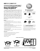


NCP1117, NCV1117
http://onsemi.com
3
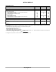
ELECTRICAL CHARACTERISTICS (C
in
= 10 mF, C
out
= 10 mF, for typical value T
A
= 25°C, for min and max values T
A
is the
operating ambient temperature range that applies unless otherwise noted. (Note 4)
Characteristic
Symbol Min Typ Max Unit
Reference Voltage, Adjustable Output Devices
(V
in
–V
out
= 2.0 V, I
out
= 10 mA, T
A
= 25°C)
(V
in
–V
out
= 1.4 V to 10 V, I
out
= 10 mA to 800 mA) (Note 4)
V
ref
1.238
1.225
1.25
−
1.262
1.270
V
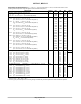
Output Voltage, Fixed Output Devices
1.5 V (V
in
= 3.5 V, I
out
= 10 mA, T
A
= 25 °C)
(V
in
= 2.9 V to 11.5 V, I
out
= 0 mA to 800 mA) (Note 4)
1.8 V (V
in
= 3.8 V, I
out
= 10 mA, T
A
= 25 °C)
(V
in
= 3.2 V to 11.8 V, I
out
= 0 mA to 800 mA) (Note 4)
1.9 V (V
in
= 3.9 V, I
out
= 10 mA, T
A
= 25 °C)
(V
in
= 3.3 V to 11.9 V, I
out
= 0 mA to 800 mA) (Note 4)
2.0 V (V
in
= 4.0 V, I
out
= 10 mA, T
A
= 25 °C)
(V
in
= 3.4 V to 12 V, I
out
= 0 mA to 800 mA) (Note 4)
2.5 V (V
in
= 4.5 V, I
out
= 10 mA, T
A
= 25 °C)
(V
in
= 3.9 V to 10 V, I
out
= 0 mA to 800 mA,) (Note 4)
2.85 V (V
in
= 4.85 V, I
out
= 10 mA, T
A
= 25 °C)
(V
in
= 4.25 V to 10 V, I
out
= 0 mA to 800 mA) (Note 4)
(V
in
= 4.0 V, I
out
= 0 mA to 500 mA) (Note 4)
3.3 V (V
in
= 5.3 V, I
out
= 10 mA, T
A
= 25 °C)
(V
in
= 4.75 V to 10 V, I
out
= 0 mA to 800 mA) (Note 4)
5.0 V (V
in
= 7.0 V, I
out
= 10 mA, T
A
= 25 °C)
(V
in
= 6.5 V to 12 V, I
out
= 0 mA to 800 mA) (Note 4)
12 V (V
in
= 14 V, I
out
= 10 mA, T
A
= 25 °C)
(V
in
= 13.5 V to 20 V, I
out
= 0 mA to 800 mA) (Note 4)
V
out
1.485
1.470
1.782
1.755
1.872
1.862
1.970
1.960
2.475
2.450
2.821
2.790
2.790
3.267
3.235
4.950
4.900
11.880
11.760
1.500
−
1.800
−
1.900
1.900
2.000
−
2.500
−
2.850
−
−
3.300
−
5.000
−
12.000
−
1.515
1.530
1.818
1.845
1.929
1.938
2.030
2.040
2.525
2.550
2.879
2.910
2.910
3.333
3.365
5.050
5.100
12.120
12.240
V
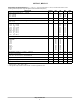
Line Regulation (Note 5) Adjustable (V
in
= 2.75 V to 16.25 V, I
out
= 10 mA) Reg
line
− 0.04 0.1 %
1.5 V (V
in
= 2.9 V to 11.5 V, I
out
= 0 mA)
1.8 V (V
in
= 3.2 V to 11.8 V, I
out
= 0 mA)
1.9 V (V
in
= 3.3 V to 11.9 V, I
out
= 0 mA)
2.0 V (V
in
= 3.4 V to 12 V, I
out
= 0 mA)
2.5 V (V
in
= 3.9 V to 10 V, I
out
= 0 mA)
2.85 V (V
in
= 4.25 V to 10 V, I
out
= 0 mA)
3.3 V (V
in
= 4.75 V to 15 V, I
out
= 0 mA)
5.0 V (V
in
= 6.5 V to 15 V, I
out
= 0 mA)
12 V (V
in
= 13.5 V to 20 V, I
out
= 0 mA)
−
−
−
−
−
−
−
−
−
0.3
0.4
0.5
0.5
0.5
0.8
0.8
0.9
1.0
1.0
1.0
2.5
2.5
2.5
3.0
4.5
6.0
7.5
mV
Load Regulation (Note 5) Adjustable (I
out
= 10 mA to 800 mA, V
in
= 4.25 V) Reg
line
− 0.2 0.4 %
1.5 V (I
out
= 0 mA to 800 mA, V
in
= 2.9 V)
1.8 V (I
out
= 0 mA to 800 mA, V
in
= 3.2 V)
1.9 V (I
out
= 0 mA to 800 mA, V
in
= 3.3 V)
2.0 V (I
out
= 0 mA to 800 mA, V
in
= 3.4 V)
2.5 V (I
out
= 0 mA to 800 mA, V
in
= 3.9 V)
2.85 V (I
out
= 0 mA to 800 mA, V
in
= 4.25 V)
3.3 V (I
out
= 0 mA to 800 mA, V
in
= 4.75 V)
5.0 V (I
out
= 0 mA to 800 mA, V
in
= 6.5 V)
12 V (I
out
= 0 mA to 800 mA, V
in
= 13.5 V)
−
−
−
−
−
−
−
−
−
2.3
2.6
2.7
3.0
3.3
3.8
4.3
6.7
16
5.5
6.0
6.0
6.0
7.5
8.0
10
15
28
mV
4. NCP1117: T
low
= 0°C , T
high
= 125°C
NCV1117: T
low
= −40°C, T
high
= 125°C
5. Low duty cycle pulse techniques are used during testing to maintain the junction temperature as close to ambient as possible.