
Data Sheet

Fully Integrated, Hall Effect-Based Linear Current Sensor IC
with 3 kVRMS Voltage Isolation and a Low-Resistance Current Conductor
ACS756
8
Allegro MicroSystems, Inc.
115 Northeast Cutoff
Worcester, Massachusetts 01615-0036 U.S.A.
1.508.853.5000; www.allegromicro.com
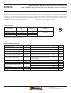
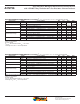
Output Voltage versus Sampled Current
Total Output Error at 0 A and at Half-Scale Current
Increasing V
IOUT
(V)
+I
P
(A)
Accuracy
Accuracy
Accuracy
25°C Only
Accuracy
25°C Only
Accuracy
25°C Only
Accuracy
0 A
vrOe $Temp erature
Average
V
IOUT
–I
P
(A)
vrOe $Temp erature
vrOe $Temp erature
Decreasing V
IOUT
(V)
I
P
(min)
I
P
(max)
Half Scale
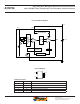
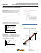
Definitions of Dynamic Response Characteristics
Propagation delay (t
PROP
). The time required for the device
output to reflect a change in the primary current signal. Propaga-
tion delay is attributed to inductive loading within the linear IC
package, as well as in the inductive loop formed by the primary
conductor geometry. Propagation delay can be considered as a
fixed time offset and may be compensated.
Primary Current
Transducer Output
90
0
I (%)
Propagation Time, t
PROP
t
Primary Current
Transducer Output
90
10
0
I (%)
Rise Time, t
r
t
Rise time (t
r
). The time interval between a) when the device
reaches 10% of its full scale value, and b) when it reaches 90%
of its full scale value. The rise time to a step response is used to
derive the bandwidth of the device, in which ƒ(–3 dB) = 0.35 / t
r
.
Both t
r
and t
RESPONSE
are detrimentally affected by eddy current
losses observed in the conductive IC ground plane.
Power-On Time (t
PO
). When the supply is ramped to its operat-
ing voltage, the device requires a finite time to power its internal
components before responding to an input magnetic field.
Power-On Time, t
PO
, is defined as the time it takes for the output
voltage to settle within ±10% of its steady state value under an
applied magnetic field, after the power supply has reached its
minimum specified operating voltage, V
CC
(min), as shown in the
chart at right.