
Data Sheet
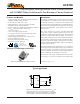

Fully Integrated, Hall Effect-Based Linear Current Sensor IC
with 3 kVRMS Voltage Isolation and a Low-Resistance Current Conductor
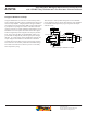
ACS756
5
Allegro MicroSystems, Inc.
115 Northeast Cutoff
Worcester, Massachusetts 01615-0036 U.S.A.
1.508.853.5000; www.allegromicro.com
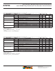
X050 PERFORMANCE CHARACTERISTICS over Range S
1
: T
OP
= –20°C to 85°C, V
CC
= 5 V, unless otherwise specified
Characteristic Symbol Test Conditions Min. Typ. Max. Units
Primary Sampled Current I
P
–50 – 50 A
Sensitivity
Sens
TA
Half scale of I
P
applied for 5 ms, T
A
= 25°C – 40 – mV/A
Sens
TOP
Half scale of I
P
applied for 5 ms 38.3 – 41.7 mV/A
Noise
2
V
NOISE
T
A
= 25°C, 10 nF on VIOUT pin to GND – 10 – mV
Nonlinearity
E
LIN(HT)
Up to full scale of I
P
, I
P
applied for 5 ms, T
OP
= 25°C to 85°C – 1 – 1 %
E
LIN(LT)
Up to full scale of I
P
, I
P
applied for 5 ms, T
OP
= –20°C to 25°C – 1 – 1 %
Electrical Offset Voltage
3
V
OE(TA)
I
P
= 0 A, T
A
= 25°C – ±2 – mV
V
OE(TOP)HT
I
P
= 0 A, T
OP
= 25°C to 85°C –30 – 30 mV
V
OE(TOP)LT
I
P
= 0 A, T
OP
= –20°C to 25°C –30 – 30 mV
Total Output Error
4
E
TOT(HT)
Over full scale of I
P
, I
P
applied for 5 ms, T
OP
= 25°C to 85°C –5 – 5 %
E
TOT(LT)
Over full scale of I
P
, I
P
applied for 5 ms, T
OP
= –20°C to 25°C –5 – 5 %
1
Device may be operated at higher primary current levels, I
P
, and ambient temperatures, T
OP
, provided that the Maximum Junction Temperature,
T
J
(max), is not exceeded.
2
6 noise voltage.
3
V
OE(TOP)
drift is referred to ideal V
OE
= 2.5 V at 0 A.
4
Percentage of I
P
, with I
P
= 25 A. Output filtered.
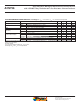
X050 PERFORMANCE CHARACTERISTICS over Range K
1
: T
OP
= –40°C to 125°C, V
CC
= 5 V, unless otherwise specified
Characteristic Symbol Test Conditions Min. Typ. Max. Units
Primary Sampled Current I
P
–50 – 50 A
Sensitivity
Sens
TA
Half scale of I
P
applied for 5 ms, T
A
= 25°C – 40 – mV/A
Sens
TOP
Half scale of I
P
applied for 5 ms 37.2 – 42.8 mV/A
Noise
2
V
NOISE
T
A
= 25°C, 10 nF on VIOUT pin to GND – 10 – mV
Nonlinearity
E
LIN(HT)
Up to full scale of I
P
, I
P
applied for 5 ms, T
OP
= 25°C to 125°C – 1 – 1 %
E
LIN(LT)
Up to full scale of I
P
, I
P
applied for 5 ms, T
OP
= –40°C to 25°C – 1.8 – 1.8 %
Electrical Offset Voltage
3
V
OE(TA)
I
P
= 0 A, T
A
= 25°C – ±2 – mV
V
OE(TOP)HT
I
P
= 0 A, T
OP
= 25°C to 125°C –30 – 30 mV
V
OE(TOP)LT
I
P
= 0 A, T
OP
= –40°C to 25°C –60 – 60 mV
Total Output Error
4
E
TOT(HT)
Over full scale of I
P
, I
P
applied for 5 ms, T
OP
= 25°C to 125°C –7.5 – 7.5 %
E
TOT(LT)
Over full scale of I
P
, I
P
applied for 5 ms, T
OP
= –40°C to 25°C –7.5 – 7.5 %
1
Device may be operated at higher primary current levels, I
P
, and ambient temperatures, T
OP
, provided that the Maximum Junction Temperature,
T
J
(max), is not exceeded.
2
6 noise voltage.
3
V
OE(TOP)
drift is referred to ideal V
OE
= 2.5 V at 0 A.
4
Percentage of I
P
, with I
P
= 25 A. Output filtered.