
AutoStore nvSRAM Specification Sheet
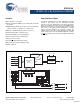
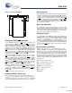
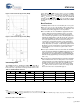
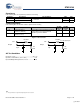
Table Of Contents
- Features
- Functional Description
- Pin Configurations
- Device Operation
- SRAM Read
- SRAM Write
- AutoStore Operation
- AutoStore Inhibit mode
- Hardware STORE (HSB) Operation
- Hardware RECALL (Power Up)
- Data Protection
- Noise Considerations
- Hardware Protect
- Low Average Active Power
- Preventing Store
- Best Practices
- Maximum Ratings
- Operating Range
- DC Electrical Characteristics
- Data Retention and Endurance
- Capacitance
- Thermal Resistance
- AC Test Conditions
- AutoStore or Power Up RECALL
- Switching Waveform
- Ordering Information
- Document History Page
- Sales, Solutions, and Legal Information
STK22C48
Document Number: 001-51000 Rev. ** Page 8 of 14
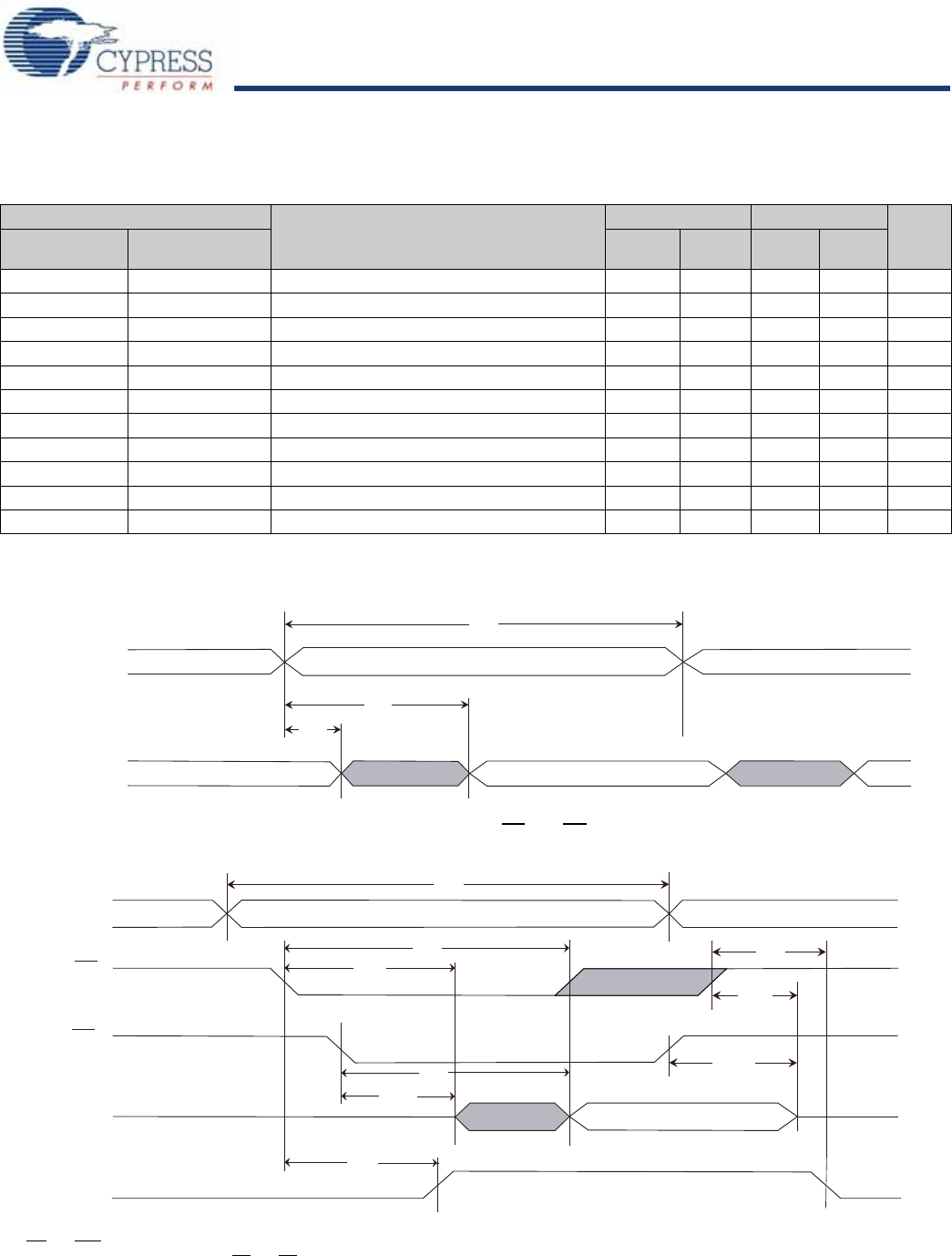
AC Switching Characteristics
SRAM Read Cycle
Parameter
Description
25 ns 45 ns
Unit
Min Max Min Max
Cypress
Parameter
Alt
t
ACE
t
ELQV
Chip Enable Access Time 25 45 ns
t
RC
[6]
t
AVAV,
t
ELEH
Read Cycle Time 25 45 ns
t
AA
[7]
t
AVQV
Address Access Time 25 45 ns
t
DOE
t
GLQV
Output Enable to Data Valid 10 20 ns
t
OHA
[7]
t
AXQX
Output Hold After Address Change 5 5 ns
t
LZCE
[8]
t
ELQX
Chip Enable to Output Active 5 5 ns
t
HZCE
[8]
t
EHQZ
Chip Disable to Output Inactive 10 15 ns
t
LZOE
[8]
t
GLQX
Output Enable to Output Active 0 0 ns
t
HZOE
[8]
t
GHQZ
Output Disable to Output Inactive 10 15 ns
t
PU
[5]
t
ELICCH
Chip Enable to Power Active 0 0 ns
t
PD
[5]
t
EHICCL
Chip Disable to Power Standby 25 45 ns
Switching Waveforms
Figure 7. SRAM Read Cycle 1: Address Controlled
[6, 7]
Figure 8. SRAM Read Cycle 2: CE and OE Controlled
[6]
W
5&
W
$$
W
2+$
$''5(66
'4'$7$287
'$7$9$/,'
$''5(66
W
5&
&(
W
$&(
W
/=&(
W
3'
W
+=&(
2(
W
'2(
W
/=2(
W
+=2(
'$7$9$/,'
$&7,9(
67$1'%<
W
38
'4'$7$287
,&&
Notes
6. WE
and HSB must be High during SRAM Read cycles.
7. Device is continuously selected with CE
and OE both Low.
8. Measured ±200 mV from steady state output voltage.
[+] Feedback