
SoftStore nvSRAM Specification Sheet
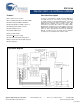
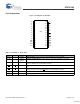
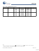
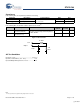
Table Of Contents
- Features
- Functional Description
- Logic Block Diagram
- Pin Configurations
- Device Operation
- SRAM Read
- SRAM Write
- Software STORE
- Software RECALL
- Hardware RECALL (Power Up)
- Hardware Protect
- Noise Considerations
- Low Average Active Power
- Best Practices
- Maximum Ratings
- Operating Range
- DC Electrical Characteristics
- Data Retention and Endurance
- Capacitance
- Thermal Resistance
- AC Test Conditions
- Switching Waveforms
- Switching Waveforms
- STORE INHIBIT or Power Up RECALL
- Switching Waveforms
- Software Controlled STORE/RECALL Cycle
- Switching Waveforms
- Part Numbering Nomenclature
- Ordering Information
- Document History Page
- Sales, Solutions and Legal Information
STK11C88
Document Number: 001-50591 Rev. ** Page 9 of 15
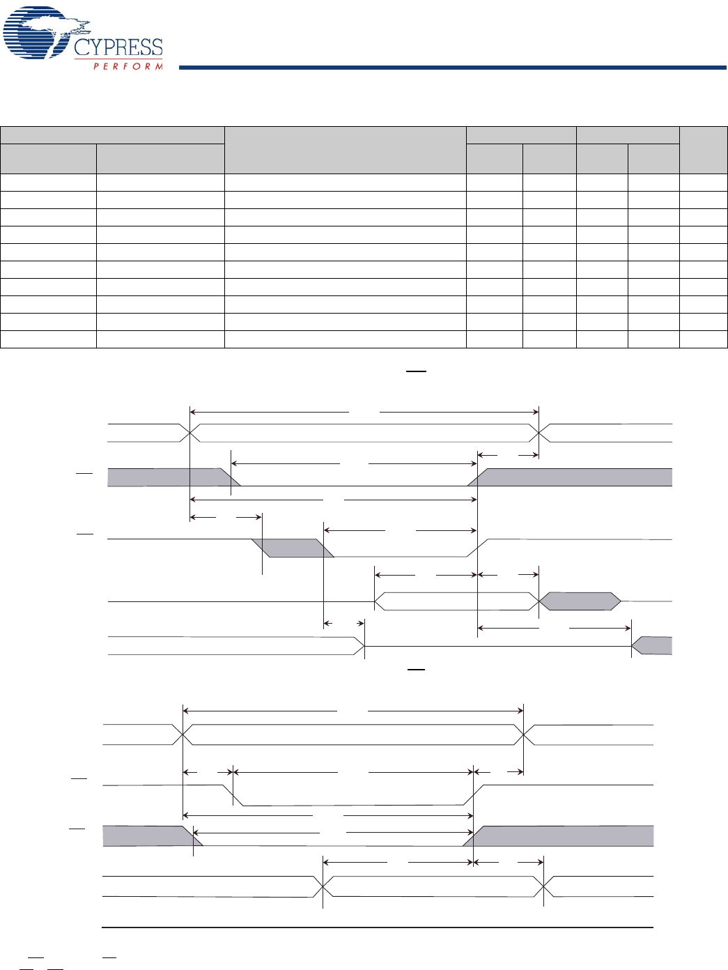
SRAM Write Cycle
Parameter
Description
25 ns 45 ns
Unit
Min Max Min Max
Cypress
Parameter
Alt
t
WC
t
AVAV
Write Cycle Time 25 45 ns
t
PWE
t
WLWH,
t
WLEH
Write Pulse Width 20 30 ns
t
SCE
t
ELWH,
t
ELEH
Chip Enable To End of Write 20 30 ns
t
SD
t
DVWH,
t
DVEH
Data Setup to End of Write 10 15 ns
t
HD
t
WHDX,
t
EHDX
Data Hold After End of Write 0 0 ns
t
AW
t
AVWH,
t
AVEH
Address Setup to End of Write 20 30 ns
t
SA
t
AVWL,
t
AVEL
Address Setup to Start of Write 0 0 ns
t
HA
t
WHAX,
t
EHAX
Address Hold After End of Write 0 0 ns
t
HZWE
[7,8]
t
WLQZ
Write Enable to Output Disable 10 15 ns
t
LZWE
[7]
t
WHQX
Output Active After End of Write 5 5 ns
Switching Waveforms
Figure 7. SRAM Write Cycle 1: WE Controlled
[9]
Figure 8. SRAM Write Cycle 2: CE Controlled
[9]
t
WC
t
SCE
t
HA
t
AW
t
SA
t
PWE
t
SD
t
HD
t
HZWE
t
LZWE
ADDRESS
CE
WE
DATA IN
DATA OUT
DATA VALID
HIGH IMPEDANCE
PREVIOUS DATA
t
WC
ADDRESS
t
SA
t
SCE
t
HA
t
AW
t
PWE
t
SD
t
HD
CE
WE
DATA IN
DATA OUT
HIGH IMPEDANCE
DATA VALID
Notes
8. If WE
is Low when CE goes Low, the outputs remain in the high impedance state.
9.
CE
or WE must be greater than V
IH
during address transitions.
[+] Feedback