
SoftStore nvSRAM Specification Sheet
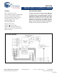
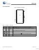
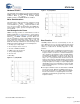
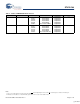
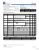
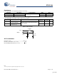
Table Of Contents
- Features
- Functional Description
- Logic Block Diagram
- Pin Configurations
- Device Operation
- SRAM Read
- SRAM Write
- Software STORE
- Software RECALL
- Hardware RECALL (Power Up)
- Hardware Protect
- Noise Considerations
- Low Average Active Power
- Best Practices
- Maximum Ratings
- Operating Range
- DC Electrical Characteristics
- Data Retention and Endurance
- Capacitance
- Thermal Resistance
- AC Test Conditions
- Switching Waveforms
- Switching Waveforms
- STORE INHIBIT or Power Up RECALL
- Switching Waveforms
- Software Controlled STORE/RECALL Cycle
- Switching Waveforms
- Part Numbering Nomenclature
- Ordering Information
- Document History Page
- Sales, Solutions and Legal Information
STK11C88
Document Number: 001-50591 Rev. ** Page 7 of 15
Capacitance
In the following table, the capacitance parameters are listed.
[4]
Parameter Description Test Conditions Max Unit
C
IN
Input Capacitance T
A
= 25°C, f = 1 MHz,
V
CC
= 0 to 3.0 V
5pF
C
OUT
Output Capacitance 7 pF
Thermal Resistance
In the following table, the thermal resistance parameters are listed.
[4]
Parameter Description Test Conditions
28-SOIC
(300 mil)
28-SOIC
(330 mil)
Unit
Θ
JA
Thermal Resistance
(Junction to Ambient)
Test conditions follow standard test methods and
procedures for measuring thermal impedance,
per EIA / JESD51.
TBD TBD °C/W
Θ
JC
Thermal Resistance
(Junction to Case)
TBD TBD °C/W
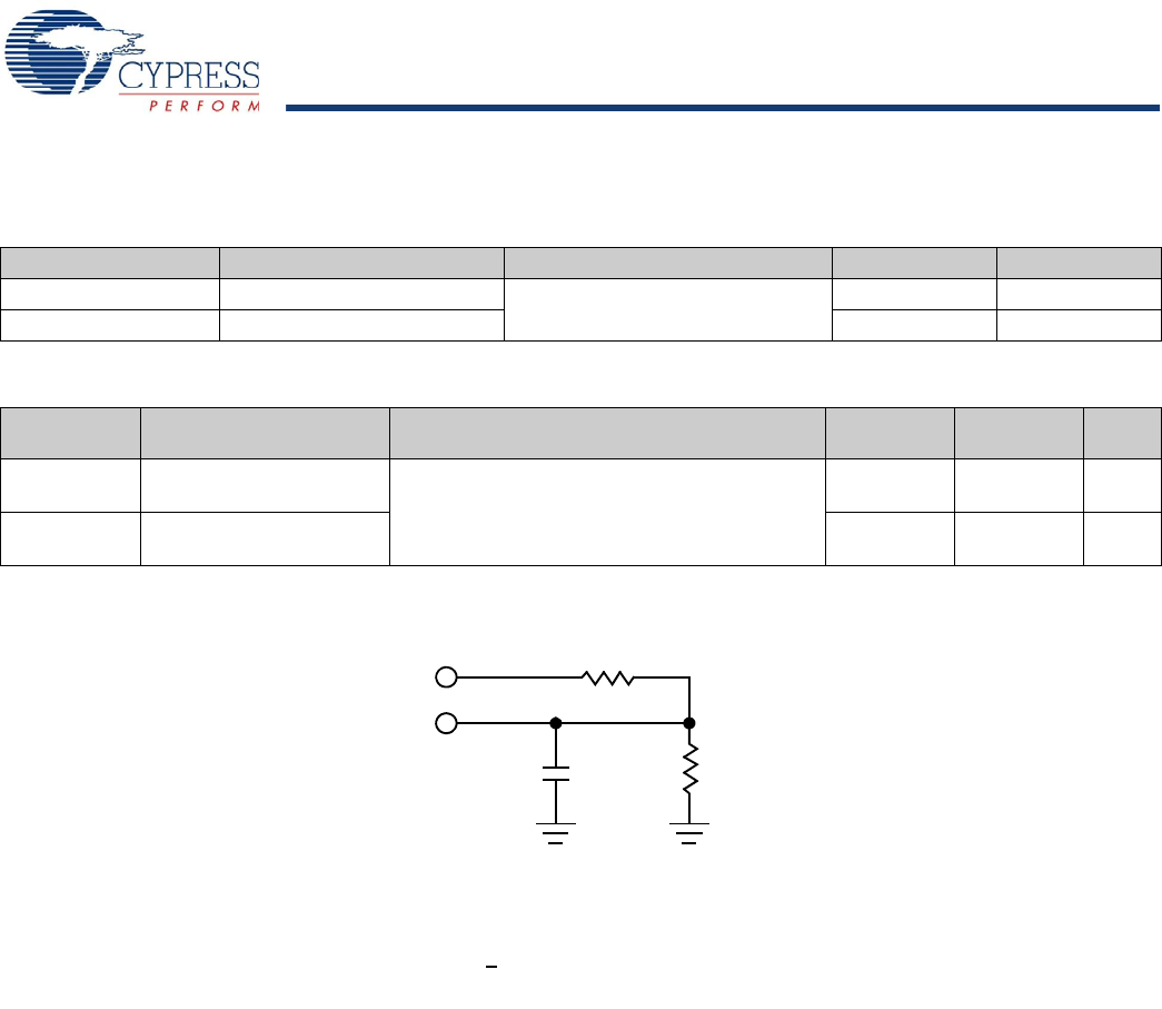
Figure 4. AC Test Loads
AC Test Conditions
5.0V
Output
30 pF
R1 480Ω
R2
255Ω
Input Pulse Levels..................................................0 V to 3 V
Input Rise and Fall Times (10% - 90%)........................ <
5 ns
Input and Output Timing Reference Levels................... 1.5 V
Note
4. These parameters are guaranteed by design and are not tested.
[+] Feedback