
SoftStore nvSRAM Specification Sheet
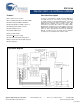
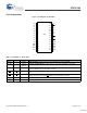
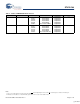
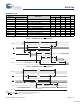
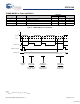
Table Of Contents
- Features
- Functional Description
- Logic Block Diagram
- Pin Configurations
- Device Operation
- SRAM Read
- SRAM Write
- Software STORE
- Software RECALL
- Hardware RECALL (Power Up)
- Hardware Protect
- Noise Considerations
- Low Average Active Power
- Best Practices
- Maximum Ratings
- Operating Range
- DC Electrical Characteristics
- Data Retention and Endurance
- Capacitance
- Thermal Resistance
- AC Test Conditions
- Switching Waveforms
- Switching Waveforms
- STORE INHIBIT or Power Up RECALL
- Switching Waveforms
- Software Controlled STORE/RECALL Cycle
- Switching Waveforms
- Part Numbering Nomenclature
- Ordering Information
- Document History Page
- Sales, Solutions and Legal Information
STK11C88
Document Number: 001-50591 Rev. ** Page 2 of 15
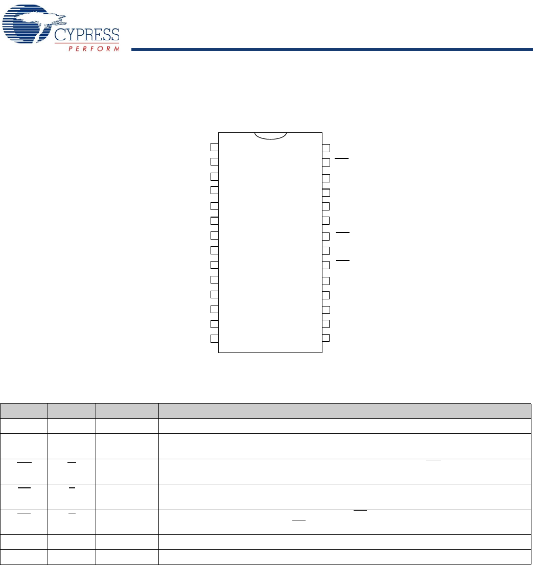
Pin Configurations
Figure 1. Pin Diagram - 28-Pin SOIC
Table 1. Pin Definitions - 28-Pin SOIC
Pin Name Alt IO Type Description
A
0
–A
14
Input Address Inputs. Used to select one of the 32,768 bytes of the nvSRAM.
DQ
0
-DQ
7
Input or
Output
Bidirectional Data IO lines. Used as input or output lines depending on operation.
WE W
Input Write Enable Input, Active LOW. When the chip is enabled and WE is LOW, data on the
IO pins is written to the specific address location.
CE
E
Input Chip Enable Input, Active LOW. When LOW, selects the chip. When HIGH, deselects the
chip.
OE
G
Input Output Enable, Active LOW. The active LOW OE input enables the data output buffers
during read cycles. Deasserting OE
HIGH causes the IO pins to tri-state.
V
SS
Ground Ground for the Device. The device is connected to the ground of the system.
V
CC
Power Supply Power Supply Inputs to the Device.
$
$
$
$
'4
'4
'4
$
$
$
$
$
$
$
$
'4
'4
9
66
$
&(
$
$
9
&&
:(
'4
'4
'4
2(
723
[+] Feedback