
Burst Architecture Specification Sheet
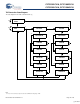
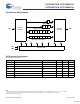
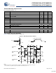
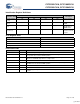

Table Of Contents
- Features
- Configurations
- Functional Description
- Selection Guide
- Logic Block Diagram (CY7C1392CV18)
- Logic Block Diagram (CY7C1992CV18)
- Logic Block Diagram (CY7C1393CV18)
- Logic Block Diagram (CY7C1394CV18)
- Pin Configuration
- Pin Definitions
- Functional Overview
- Application Example
- Truth Table
- Write Cycle Descriptions
- Write Cycle Descriptions
- Write Cycle Descriptions
- IEEE 1149.1 Serial Boundary Scan (JTAG)
- TAP Controller State Diagram
- TAP Controller Block Diagram
- TAP Electrical Characteristics
- TAP AC Switching Characteristics
- TAP Timing and Test Conditions
- Identification Register Definitions
- Scan Register Sizes
- Instruction Codes
- Boundary Scan Order
- Power Up Sequence in DDR-II SRAM
- Maximum Ratings
- Operating Range
- Electrical Characteristics
- Capacitance
- Thermal Resistance
- Switching Characteristics
- Switching Waveforms
- Ordering Information
- Package Diagram
- Document History Page
- Sales, Solutions, and Legal Information
CY7C1392CV18, CY7C1992CV18
CY7C1393CV18, CY7C1394CV18
Document #: 001-07162 Rev. *C Page 15 of 30
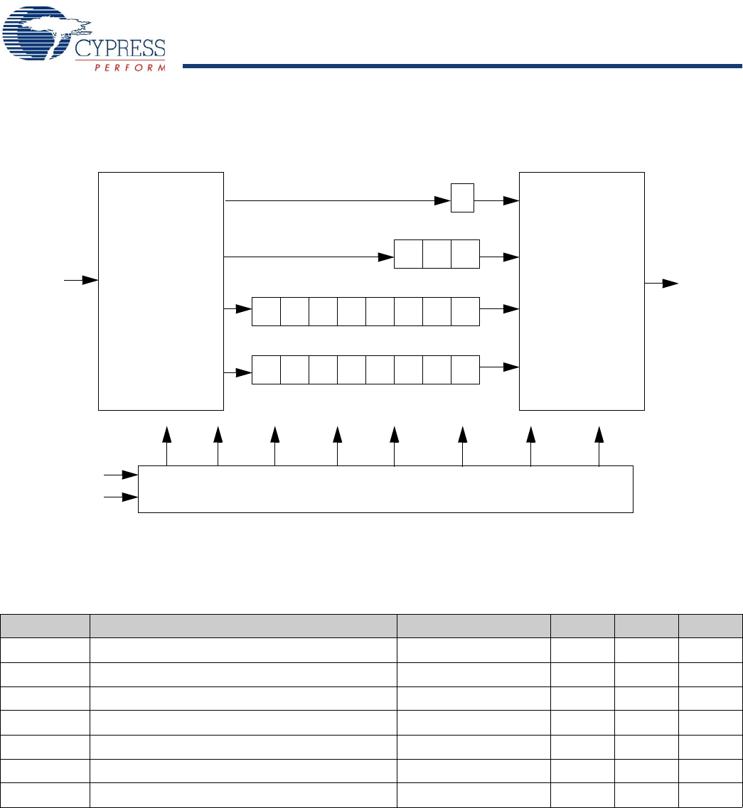
TAP Controller Block Diagram
TAP Electrical Characteristics
Over the Operating Range
[10, 11, 12]
Parameter Description Test Conditions Min Max Unit
V
OH1
Output HIGH Voltage I
OH
= −2.0 mA 1.4 V
V
OH2
Output HIGH Voltage I
OH
= −100 μA1.6 V
V
OL1
Output LOW Voltage I
OL
= 2.0 mA 0.4 V
V
OL2
Output LOW Voltage I
OL
= 100 μA0.2V
V
IH
Input HIGH Voltage 0.65V
DD
V
DD
+ 0.3 V
V
IL
Input LOW Voltage –0.3 0.35V
DD
V
I
X
Input and Output Load Current GND ≤ V
I
≤ V
DD
–5 5 μA
0
012..29
3031
Boundary Scan Register
Identification Register
012..
.
.106
012
Instruction Register
Bypass Register
Selection
Circuitry
Selection
Circuitry
TAP Controller
TDI
TDO
TCK
TMS
Notes
10. These characteristics pertain to the TAP inputs (TMS, TCK, TDI and TDO). Parallel load levels are specified in the Electrical Characteristics table.
11. Overshoot: V
IH
(AC) < V
DDQ
+ 0.85V (Pulse width less than t
CYC
/2), Undershoot: V
IL
(AC) > −1.5V (Pulse width less than t
CYC
/2).
12. All Voltage referenced to Ground.
[+] Feedback