
Synchronous Dual-Port RAM Specification Sheet

CY7C0850AV, CY7C0851AV
CY7C0852AV, CY7C0853AV
Document #: 38-06070 Rev. *H Page 18 of 32
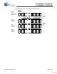
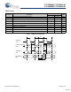
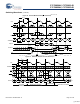
Figure 10. Bank Select Read
[26, 27]
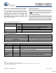
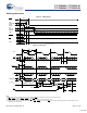
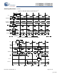
Figure 11. Read-to-Write-to-Read (OE = LOW)
[25, 28, 29, 30, 31]
Switching Waveforms (continued)
Q
3
Q
1
Q
0
Q
2
A
0
A
1
A
2
A
3
A
4
A
5
Q
4
A
0
A
1
A
2
A
3
A
4
A
5
t
SA
t
HA
t
SC
t
HC
t
SA
t
HA
t
SC
t
HC
t
SC
t
HC
t
SC
t
HC
t
CKHZ
t
DC
t
DC
t
CD2
t
CKLZ
t
CD2
t
CD2
t
CKHZ
t
CKLZ
t
CD2
t
CKHZ
t
CKLZ
t
CD2
t
CH2
t
CL2
t
CYC2
CLK
ADDRESS
(B1)
CE
(B1)
DATA
OUT(B2)
DATA
OUT(B1)
ADDRESS
(B2)
CE
(B2)
t
CYC2
t
CL2
t
CH2
t
HC
t
SC
t
HW
t
SW
t
HA
t
SA
t
HW
t
SW
t
CD2
t
CKHZ
t
SD
t
HD
NO
OPERATION WRITEREAD READ
CLK
CE
R/W
ADDRESS
DATA
IN
DATA
OUT
A
n
A
n+1
A
n+2
A
n+2
D
n+2
A
n+3
A
n+4
Q
n
Q
n+3
Q
n+1
t
CD2
t
CD2
t
CKLZ
Notes
26. In this depth-expansion example, B1 represents Bank #1 and B2 is Bank #2; each bank consists of one Cypress CY7C0851AV/CY7C0852AV device from this data
sheet. ADDRESS
(B1)
= ADDRESS
(B2)
.
27. ADS
= CNTEN= B0 – B3 = OE = LOW; MRST = CNTRST = CNT/MSK = HIGH.
28. Output state (HIGH, LOW, or high-impedance) is determined by the previous cycle control signals.
29. During “No Operation,” data in memory at the selected address may be corrupted and should be rewritten to ensure data integrity.
30. CE
0
= OE = B0 – B3 = LOW; CE
1
= R/W = CNTRST = MRST = HIGH.
31. CE
0
= B0 – B3 = R/W = LOW; CE
1
= CNTRST = MRST = CNT/MSK = HIGH. When R/W first switches low, since OE = LOW, the Write operation cannot be completed
(labelled as no operation). One clock cycle is required to three-state the I/O for the Write operation on the next rising edge of CLK.
[+] Feedback