
Programmable Embedded USB Host and Peripheral Controller with Automotive AEC Grade Support Specification Sheet
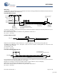
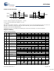
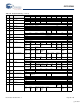
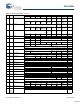
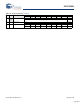
Table Of Contents
- EZ-Host Features
- Typical Applications
- Introduction
- Functional Overview
- Interface Descriptions
- USB Interface
- OTG Interface
- External Memory Interface
- General Purpose IO Interface (GPIO)
- UART Interface
- I2C EEPROM Interface
- Serial Peripheral Interface
- High-Speed Serial Interface
- Programmable Pulse/PWM Interface
- Host Port Interface
- IDE Interface
- Charge Pump Interface
- Booster Interface
- Crystal Interface
- Boot Configuration Interface
- Operational Modes
- Power Savings and Reset Description
- Memory Map
- Registers
- Processor Control Registers
- CPU Flags Register [0xC000] [R]
- Bank Register [0xC002] [R/W]
- Hardware Revision Register [0xC004] [R]
- CPU Speed Register [0xC008] [R/W]
- Power Control Register [0xC00A] [R/W]
- Interrupt Enable Register [0xC00E] [R/W]
- Breakpoint Register [0xC014] [R/W]
- USB Diagnostic Register [0xC03C] [R/W]
- Memory Diagnostic Register [0xC03E] [W]
- External Memory Registers
- Timer Registers
- General USB Registers
- USB Host Only Registers
- Host n Control Register [R/W]
- Host n Address Register [R/W]
- Host n Count Register [R/W]
- Host n Endpoint Status Register [R]
- Host n PID Register [W]
- Host n Count Result Register [R]
- Host n Device Address Register [W]
- Host n Interrupt Enable Register [R/W]
- Host n Status Register [R/W]
- Host n SOF/EOP Count Register [R/W]
- Host n SOF/EOP Counter Register [R]
- Host n Frame Register [R]
- USB Device Only Registers
- Device n Endpoint n Control Register [R/W]
- Device n Endpoint n Address Register [R/W]
- Device n Endpoint n Count Register [R/W]
- Device n Endpoint n Status Register [R/W]
- Device n Endpoint n Count Result Register [R/W]
- Device n Port Select Register [R/W]
- Device n Interrupt Enable Register [R/W]
- Device n Address Register [W]
- Device n Status Register [R/W]
- Device n Frame Number Register [R]
- Device n SOF/EOP Count Register [W]
- OTG Control Registers
- GPIO Registers
- IDE Registers
- HSS Registers
- HSS Control Register [0xC070] [R/W]
- HSS Baud Rate Register [0xC072] [R/W]
- HSS Transmit Gap Register [0xC074] [R/W]
- HSS Data Register [0xC076] [R/W]
- HSS Receive Address Register [0xC078] [R/W]
- HSS Receive Counter Register [0xC07A] [R/W]
- HSS Transmit Address Register [0xC07C] [R/W]
- HSS Transmit Counter Register [0xC07E] [R/W]
- HPI Registers
- SPI Registers
- SPI Configuration Register [0xC0C8] [R/W]
- SPI Control Register [0xC0CA] [R/W]
- SPI Interrupt Enable Register [0xC0CC] [R/W]
- SPI Status Register [0xC0CE] [R]
- SPI Interrupt Clear Register [0xC0D0] [W]
- SPI CRC Control Register [0xC0D2] [R/W]
- SPI CRC Value Register [0xC0D4] [R/W]
- SPI Data Register [0xC0D6] [R/W]
- SPI Transmit Address Register [0xC0D8] [R/W]
- SPI Transmit Count Register [0xC0DA] [R/W]
- SPI Receive Address Register [0xC0DC [R/W]
- SPI Receive Count Register [0xC0DE] [R/W]
- UART Registers
- PWM Registers
- Processor Control Registers
- Pin Diagram
- Pin Descriptions
- Absolute Maximum Ratings
- Operating Conditions
- Crystal Requirements (XTALIN, XTALOUT)
- DC Characteristics
- AC Timing Characteristics
- Register Summary
- Ordering Information
- Package Diagrams
- Document History Page
- Sales, Solutions, and Legal Information
CY7C67300
Document #: 38-08015 Rev. *J Page 92 of 99
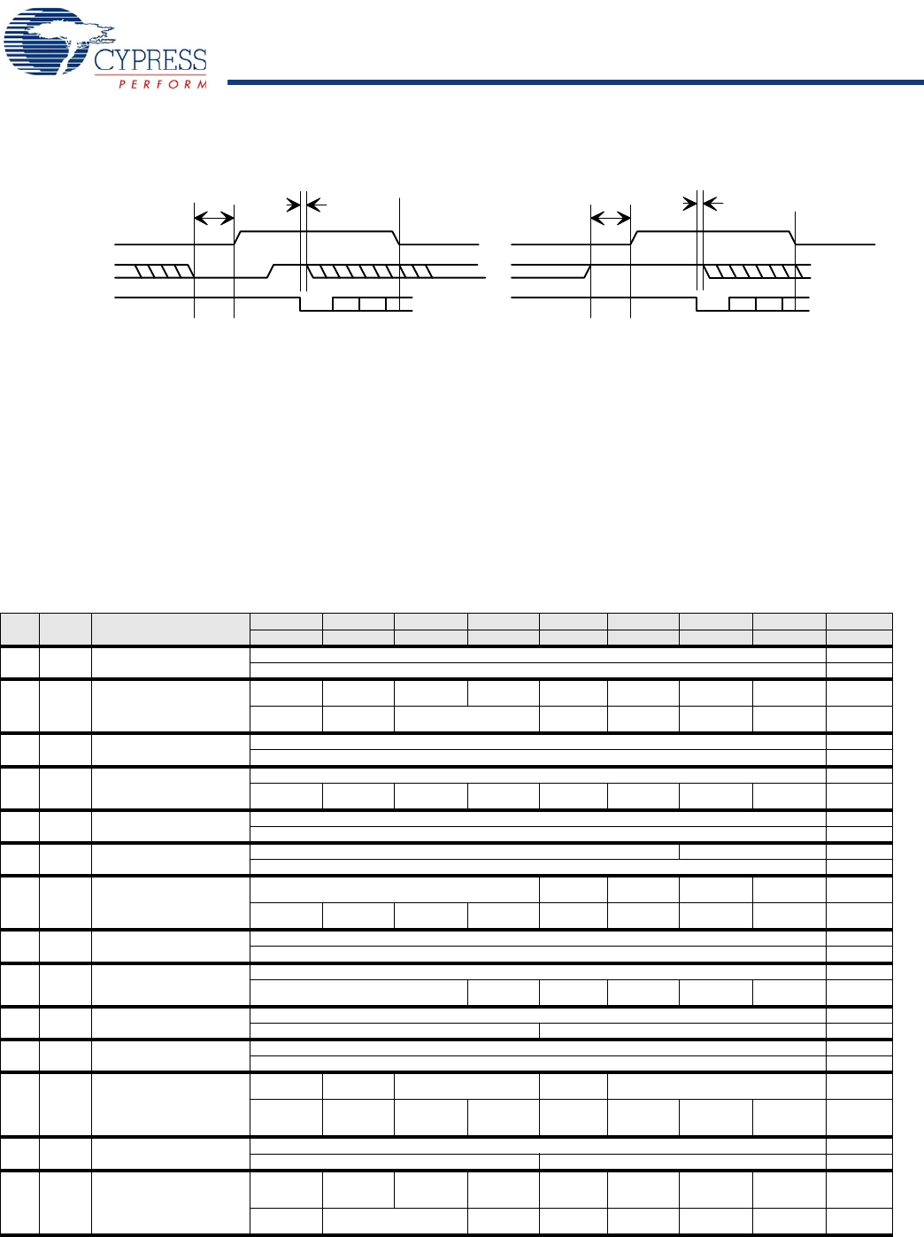
Hardware CTS/RTS Handshake
t
CTSsetup
: HSS_CTS setup time before HSS_RTS = 1.5T min.
t
CTShold
: HSS_CTS hold time after START bit = 0 ns min.
T = 1/48 MHz.
When RTS/CTS hardware handshake is enabled, transmission can be help off by deasserting HSS_CTS at least 1.5T before
HSS_RTS. Transmission resumes when HSS_CTS returns HIGH. HSS_CTS must remain HIGH until START bit.
HSS_RTS is deasserted in the third data bit time.
An application may choose to hold HSS_CTS until HSS_RTS is deasserted, which always occurs after the START bit.
Register Summary
tCTSsetup
tCTSsetup
Start of transmission delayed until HSS_CTS goes high
Start of transmission not delayed by HSS_CTS
tCTShold
tCTShold
HSS_RTS
HSS_CTS
HSS_TxD
Table 142. Register Summary
R/W Address Register Bit 15 Bit 14 Bit 13 Bit 12 Bit 11 Bit 10 Bit 9 Bit 8 Default High
Bit 7 Bit 6 Bit 5 Bit 4 Bit 3 Bit 2 Bit 1 Bit 0 Default Low
R 0x0140 HPI Breakpoint Address... 0000 0000
...Address 0000 0000
R 0x0142 Interrupt Routing VBUS to HPI
Enable
ID to HPI
Enable
SOF/EOP2 to
HPI Enable
SOF/EOP2 to
CPU Enable
SOF/EOP1 to
HPI Enable
SOF/EOP1 to
CPU Enable
Reset2 to HPI
Enable
HPI Swap 1
Enable
0001 0100
Resume2 to
HPI Enable
Resume1 to
HPI Enable
Reserved Done2 to HPI
Enable
Done1 to HPI
Enable
Reset1 to HPI
Enable
HPI Swap 0
Enable
0000 0000
W 1: 0x0144
2: 0x0148
SIEXmsg Data... xxxx xxxx
...Data xxxx xxxx
R/W 0x02n0 Device n Endpoint n Control Reserved xxxx xxxx
IN/OUT
Ignore Enable
Sequence
Select
Stall
Enable
ISO
Enable
NAK Interrupt
Enable
Direction
Select
Enable ARM
Enable
xxxx xxxx
R/W 0x02n2 Device n Endpoint n Address Address... xxxx xxxx
...Address xxxx xxxx
R.W 0x02n4 Device n Endpoint n Count Reserved Count... xxxx xxxx
...Count xxxx xxxx
R/W 0x02n6 Device n Endpoint n Status Reserved Overflow
Flag
Underflow
Flag
OUT
Exception Flag
IN
Exception Flag
xxxx xxxx
Stall
Flag
NAK
Flag
Length
Exception Flag
Setup
Flag
Sequence
Status
Timeout
Flag
Error
Flag
ACK
Flag
xxxx xxxx
R/W 0x02n8 Device n Endpoint n Count Result Result... xxxx xxxx
...Result xxxx xxxx
R 0xC000 CPU Flags Reserved... 0000 0000
...Reserved Global Inter-
rupt Enable
Negative
Flag
Overflow
Flag
Carry
Flag
Zero
Flag
000x xxxx
R/W 0xC002 Bank Address... 0000 0001
...Address Reserved 000x xxxx
R 0xC004 Hardware Revision Revision... xxxx xxxx
...Revision xxxx xxxx
R/W 0xC006 GPIO Control Write Protect
Enable
UD Reserved SAS
Enable
Mode
Select
0000 0000
HSS
Enable
HSS XD
Enable
SPI
Enable
SPI XD
Enable
Interrupt 1
Polarity
Select
Interrupt 1
Enable
Interrupt 0
Polarity
Select
Interrupt 0
Enable
0000 0000
R/W 0xC008 CPU Speed Reserved... 0000 0000
.Reserved CPU Speed 0000 1111
R/W 0xC00A Power Control Host/Device
2B Wake
Enable
Host/Device
2A Wake
Enable
Host/Device
1B Wake
Enable
Host/Device
1A Wake
Enable
OTG
Wake
Enable
Reserved HSS
Wake
Enable
SPI
Wake
Enable
0000 0000
HPI
Wake Enable
Reserved GPI
Wake Enable
Reserved Boost 3V
OK
Sleep
Enable
Halt
Enable
0000 0000
[+] Feedback