
Programmable Embedded USB Host and Peripheral Controller with Automotive AEC Grade Support Specification Sheet
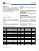
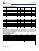
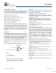
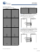
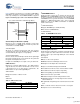
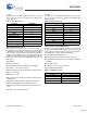
Table Of Contents
- EZ-Host Features
- Typical Applications
- Introduction
- Functional Overview
- Interface Descriptions
- USB Interface
- OTG Interface
- External Memory Interface
- General Purpose IO Interface (GPIO)
- UART Interface
- I2C EEPROM Interface
- Serial Peripheral Interface
- High-Speed Serial Interface
- Programmable Pulse/PWM Interface
- Host Port Interface
- IDE Interface
- Charge Pump Interface
- Booster Interface
- Crystal Interface
- Boot Configuration Interface
- Operational Modes
- Power Savings and Reset Description
- Memory Map
- Registers
- Processor Control Registers
- CPU Flags Register [0xC000] [R]
- Bank Register [0xC002] [R/W]
- Hardware Revision Register [0xC004] [R]
- CPU Speed Register [0xC008] [R/W]
- Power Control Register [0xC00A] [R/W]
- Interrupt Enable Register [0xC00E] [R/W]
- Breakpoint Register [0xC014] [R/W]
- USB Diagnostic Register [0xC03C] [R/W]
- Memory Diagnostic Register [0xC03E] [W]
- External Memory Registers
- Timer Registers
- General USB Registers
- USB Host Only Registers
- Host n Control Register [R/W]
- Host n Address Register [R/W]
- Host n Count Register [R/W]
- Host n Endpoint Status Register [R]
- Host n PID Register [W]
- Host n Count Result Register [R]
- Host n Device Address Register [W]
- Host n Interrupt Enable Register [R/W]
- Host n Status Register [R/W]
- Host n SOF/EOP Count Register [R/W]
- Host n SOF/EOP Counter Register [R]
- Host n Frame Register [R]
- USB Device Only Registers
- Device n Endpoint n Control Register [R/W]
- Device n Endpoint n Address Register [R/W]
- Device n Endpoint n Count Register [R/W]
- Device n Endpoint n Status Register [R/W]
- Device n Endpoint n Count Result Register [R/W]
- Device n Port Select Register [R/W]
- Device n Interrupt Enable Register [R/W]
- Device n Address Register [W]
- Device n Status Register [R/W]
- Device n Frame Number Register [R]
- Device n SOF/EOP Count Register [W]
- OTG Control Registers
- GPIO Registers
- IDE Registers
- HSS Registers
- HSS Control Register [0xC070] [R/W]
- HSS Baud Rate Register [0xC072] [R/W]
- HSS Transmit Gap Register [0xC074] [R/W]
- HSS Data Register [0xC076] [R/W]
- HSS Receive Address Register [0xC078] [R/W]
- HSS Receive Counter Register [0xC07A] [R/W]
- HSS Transmit Address Register [0xC07C] [R/W]
- HSS Transmit Counter Register [0xC07E] [R/W]
- HPI Registers
- SPI Registers
- SPI Configuration Register [0xC0C8] [R/W]
- SPI Control Register [0xC0CA] [R/W]
- SPI Interrupt Enable Register [0xC0CC] [R/W]
- SPI Status Register [0xC0CE] [R]
- SPI Interrupt Clear Register [0xC0D0] [W]
- SPI CRC Control Register [0xC0D2] [R/W]
- SPI CRC Value Register [0xC0D4] [R/W]
- SPI Data Register [0xC0D6] [R/W]
- SPI Transmit Address Register [0xC0D8] [R/W]
- SPI Transmit Count Register [0xC0DA] [R/W]
- SPI Receive Address Register [0xC0DC [R/W]
- SPI Receive Count Register [0xC0DE] [R/W]
- UART Registers
- PWM Registers
- Processor Control Registers
- Pin Diagram
- Pin Descriptions
- Absolute Maximum Ratings
- Operating Conditions
- Crystal Requirements (XTALIN, XTALOUT)
- DC Characteristics
- AC Timing Characteristics
- Register Summary
- Ordering Information
- Package Diagrams
- Document History Page
- Sales, Solutions, and Legal Information
CY7C67300
Document #: 38-08015 Rev. *J Page 9 of 99
Host Port Interface
EZ-Host has an HPI interface. The HPI interface provides DMA
access to the EZ-Host internal memory by an external host, plus
a bidirectional mailbox register for supporting high level commu-
nication protocols. This port is designed to be the primary
high-speed connection to a host processor. Complete control of
EZ-Host can be accomplished through this interface via an
extensible API and communication protocol. Other than the
hardware communication protocols, a host processor has
identical control over EZ-Host whether connecting to the HPI or
HSS port. The HPI interface is exposed through GPIO pins.
HPI Features
■ 16-bit data bus interface
■ 16 MB/s throughput
■ Auto-increment of address pointer for fast block mode transfers
■ Direct memory access (DMA) to internal memory
■ Bidirectional Mailbox register
■ Byte swapping
■ Complete access to internal memory
■ Complete control of SIEs through HPI
■ Dedicated HPI status register
HPI Pins
The two HPI address pins are used to address one of four
possible HPI port registers as shown in Table 13.
IDE Interface
EZ-Host has an IDE interface. The IDE interface supports PIO
mode 0-4 as specified in the Information Technology-AT
Attachment–4 with Packet Interface Extension (ATA/ATAPI-4)
Specification, T13/1153D Rev 18. There is no need for firmware
to use programmable wait states. The CPU read/write cycle is
automatically extended as needed for direct CPU to IDE
read/write accesses.
The EZ-Host IDE interface also has a BLOCK transfer mode that
allows EZ-Host to read/write large blocks of data to/from the IDE
data register and move it to/from the EZ-Host on-chip memory
directly without intervention of the CPU. The IDE interface is
exposed through GPIO pins. Table 14 on page 10 lists the
achieved throughput for maximum block mode data transfer rate
(with IDE_IORDY true) for the various IDE PIO modes.
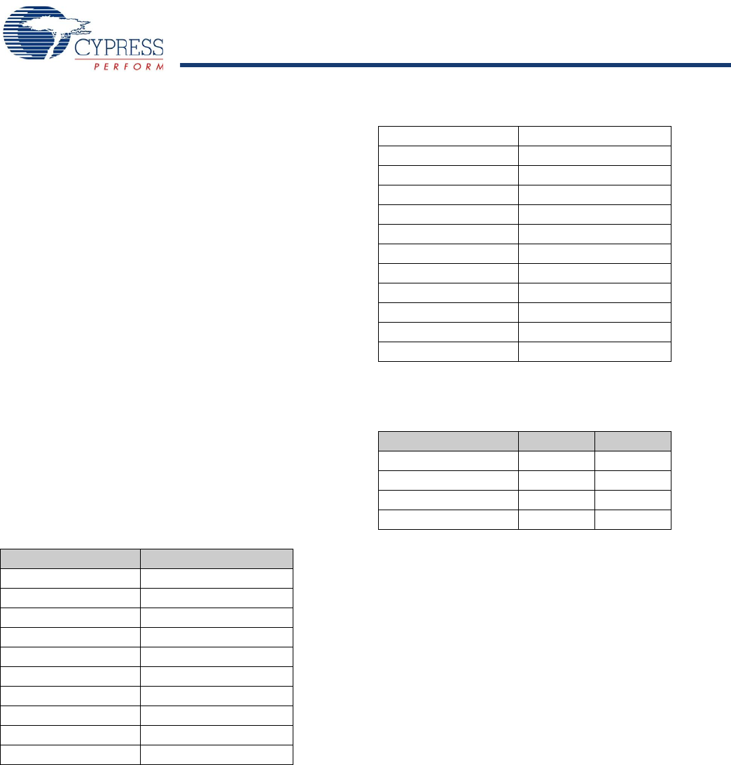
Table 12. HPI Interface Pins
[3, 4]
Pin Name Pin Number
INT 46
nRD 47
nWR 48
nCS 49
A1 50
A0 52
D15 56
D14 57
D13 58
D12 59
Notes
3. HPI_INT is for the Outgoing Mailbox interrupt.
4. HPI strobes are negative logic sampled on rising edge.
D11 60
D10 61
D9 65
D8 66
D7 86
D6 87
D5 89
D4 90
D3 91
D2 92
D1 93
D0 94
Table 13. HPI Addressing
HPI A[1:0] A1 A0
HPI Data 0 0
HPI Mailbox 0 1
HPI Address 1 0
HPI Status 1 1
Table 12. HPI Interface Pins (continued)
[3, 4]
[+] Feedback