
Programmable Embedded USB Host and Peripheral Controller with Automotive AEC Grade Support Specification Sheet
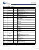
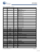
Table Of Contents
- EZ-Host Features
- Typical Applications
- Introduction
- Functional Overview
- Interface Descriptions
- USB Interface
- OTG Interface
- External Memory Interface
- General Purpose IO Interface (GPIO)
- UART Interface
- I2C EEPROM Interface
- Serial Peripheral Interface
- High-Speed Serial Interface
- Programmable Pulse/PWM Interface
- Host Port Interface
- IDE Interface
- Charge Pump Interface
- Booster Interface
- Crystal Interface
- Boot Configuration Interface
- Operational Modes
- Power Savings and Reset Description
- Memory Map
- Registers
- Processor Control Registers
- CPU Flags Register [0xC000] [R]
- Bank Register [0xC002] [R/W]
- Hardware Revision Register [0xC004] [R]
- CPU Speed Register [0xC008] [R/W]
- Power Control Register [0xC00A] [R/W]
- Interrupt Enable Register [0xC00E] [R/W]
- Breakpoint Register [0xC014] [R/W]
- USB Diagnostic Register [0xC03C] [R/W]
- Memory Diagnostic Register [0xC03E] [W]
- External Memory Registers
- Timer Registers
- General USB Registers
- USB Host Only Registers
- Host n Control Register [R/W]
- Host n Address Register [R/W]
- Host n Count Register [R/W]
- Host n Endpoint Status Register [R]
- Host n PID Register [W]
- Host n Count Result Register [R]
- Host n Device Address Register [W]
- Host n Interrupt Enable Register [R/W]
- Host n Status Register [R/W]
- Host n SOF/EOP Count Register [R/W]
- Host n SOF/EOP Counter Register [R]
- Host n Frame Register [R]
- USB Device Only Registers
- Device n Endpoint n Control Register [R/W]
- Device n Endpoint n Address Register [R/W]
- Device n Endpoint n Count Register [R/W]
- Device n Endpoint n Status Register [R/W]
- Device n Endpoint n Count Result Register [R/W]
- Device n Port Select Register [R/W]
- Device n Interrupt Enable Register [R/W]
- Device n Address Register [W]
- Device n Status Register [R/W]
- Device n Frame Number Register [R]
- Device n SOF/EOP Count Register [W]
- OTG Control Registers
- GPIO Registers
- IDE Registers
- HSS Registers
- HSS Control Register [0xC070] [R/W]
- HSS Baud Rate Register [0xC072] [R/W]
- HSS Transmit Gap Register [0xC074] [R/W]
- HSS Data Register [0xC076] [R/W]
- HSS Receive Address Register [0xC078] [R/W]
- HSS Receive Counter Register [0xC07A] [R/W]
- HSS Transmit Address Register [0xC07C] [R/W]
- HSS Transmit Counter Register [0xC07E] [R/W]
- HPI Registers
- SPI Registers
- SPI Configuration Register [0xC0C8] [R/W]
- SPI Control Register [0xC0CA] [R/W]
- SPI Interrupt Enable Register [0xC0CC] [R/W]
- SPI Status Register [0xC0CE] [R]
- SPI Interrupt Clear Register [0xC0D0] [W]
- SPI CRC Control Register [0xC0D2] [R/W]
- SPI CRC Value Register [0xC0D4] [R/W]
- SPI Data Register [0xC0D6] [R/W]
- SPI Transmit Address Register [0xC0D8] [R/W]
- SPI Transmit Count Register [0xC0DA] [R/W]
- SPI Receive Address Register [0xC0DC [R/W]
- SPI Receive Count Register [0xC0DE] [R/W]
- UART Registers
- PWM Registers
- Processor Control Registers
- Pin Diagram
- Pin Descriptions
- Absolute Maximum Ratings
- Operating Conditions
- Crystal Requirements (XTALIN, XTALOUT)
- DC Characteristics
- AC Timing Characteristics
- Register Summary
- Ordering Information
- Package Diagrams
- Document History Page
- Sales, Solutions, and Legal Information
CY7C67300
Document #: 38-08015 Rev. *J Page 84 of 99
USB Transceiver
USB 2.0 certified in full- and low-speed modes.
I
SLEEP
Sleep Current USB Peripheral: includes 1.5K
internal pull up
210 500 μA
Without 1.5K internal pull up 5 30
μA
I
SLEEPB
Sleep Current with Booster Enabled USB Peripheral: includes 1.5K
internal pull up
190 500 μA
Without 1.5K internal pull up 5 30
μA
Table 133. DC Characteristics (continued)
[8]
Parameter Description Conditions Min Typ. Max Unit
Notes
9. I
CC
and I
CCB
values are the same regardless of USB host or peripheral configuration.
10. There is no appreciable difference in I
CC
and I
CCB
values when only two transceivers are powered.
Table 134. DC Characteristics: Charge Pump
Parameter Description Conditions Min Typ. Max Unit
V
A_VBUS_OUT
Regulated OTGVBUS Voltage 8 mA< I
LOAD
< 10 mA 4.4 5.25 V
T
A_VBUS_RISE
V
BUS
Rise Time I
LOAD
= 10 mA 100 ms
I
A_VBUS_OUT
Maximum Load Current 8 10 mA
C
DRD_VBUS
OUTVBUS Bypass Capacitance 4.4V< V
BUS
< 5.25V 1.0 6.5 pF
V
A_VBUS_LKG
OTGVBUS Leakage Voltage OTGVBUS not driven 200 mV
V
DRD_DATA_LKG
Dataline Leakage Voltage 342 mV
I
CHARGE
Charge Pump Current Draw I
LOAD
= 8 mA 20 20 mA
I
LOAD
= 0 mA 0 1 mA
I
CHARGEB
Charge Pump Current Draw with
Booster Active
I
LOAD
= 8 mA 30 45 mA
I
LOAD
= 0 mA 0 5 mA
I
B_DSCHG_IN
B-Device (SRP Capable) Discharge
Current
0V< V
BUS
< 5.25V 8 mA
V
A_VBUS_VALID
A-Device VBUS Valid 4.4 V
V
A_SESS_VALID
A-Device Session Valid 0.8 2.0 V
V
B_SESS_VALID
B-Device Session Valid 0.8 4.0 V
V
A_SESS_END
B-Device Session End 0.2 0.8 V
E Efficiency When Loaded I
LOAD
= 8 mA, V
CC
= 3.3V 75 %
R
PD
Data Line Pull Down 14.25 24.8 Ω
R
A_BUS_IN
A-device V
BUS
Input Impedance to
GND
V
BUS
is not being driven 40 100 kΩ
R
B_SRP_UP
B-device V
BUS
SRP Pull Up Pull up voltage = 3.0V 281 Ω
R
B_SRP_DWN
B-device V
BUS
SRP Pull Down 656 Ω
[+] Feedback