
Programmable Embedded USB Host and Peripheral Controller with Automotive AEC Grade Support Specification Sheet
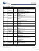
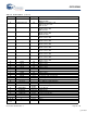
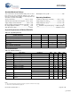
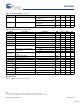
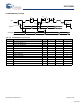
Table Of Contents
- EZ-Host Features
- Typical Applications
- Introduction
- Functional Overview
- Interface Descriptions
- USB Interface
- OTG Interface
- External Memory Interface
- General Purpose IO Interface (GPIO)
- UART Interface
- I2C EEPROM Interface
- Serial Peripheral Interface
- High-Speed Serial Interface
- Programmable Pulse/PWM Interface
- Host Port Interface
- IDE Interface
- Charge Pump Interface
- Booster Interface
- Crystal Interface
- Boot Configuration Interface
- Operational Modes
- Power Savings and Reset Description
- Memory Map
- Registers
- Processor Control Registers
- CPU Flags Register [0xC000] [R]
- Bank Register [0xC002] [R/W]
- Hardware Revision Register [0xC004] [R]
- CPU Speed Register [0xC008] [R/W]
- Power Control Register [0xC00A] [R/W]
- Interrupt Enable Register [0xC00E] [R/W]
- Breakpoint Register [0xC014] [R/W]
- USB Diagnostic Register [0xC03C] [R/W]
- Memory Diagnostic Register [0xC03E] [W]
- External Memory Registers
- Timer Registers
- General USB Registers
- USB Host Only Registers
- Host n Control Register [R/W]
- Host n Address Register [R/W]
- Host n Count Register [R/W]
- Host n Endpoint Status Register [R]
- Host n PID Register [W]
- Host n Count Result Register [R]
- Host n Device Address Register [W]
- Host n Interrupt Enable Register [R/W]
- Host n Status Register [R/W]
- Host n SOF/EOP Count Register [R/W]
- Host n SOF/EOP Counter Register [R]
- Host n Frame Register [R]
- USB Device Only Registers
- Device n Endpoint n Control Register [R/W]
- Device n Endpoint n Address Register [R/W]
- Device n Endpoint n Count Register [R/W]
- Device n Endpoint n Status Register [R/W]
- Device n Endpoint n Count Result Register [R/W]
- Device n Port Select Register [R/W]
- Device n Interrupt Enable Register [R/W]
- Device n Address Register [W]
- Device n Status Register [R/W]
- Device n Frame Number Register [R]
- Device n SOF/EOP Count Register [W]
- OTG Control Registers
- GPIO Registers
- IDE Registers
- HSS Registers
- HSS Control Register [0xC070] [R/W]
- HSS Baud Rate Register [0xC072] [R/W]
- HSS Transmit Gap Register [0xC074] [R/W]
- HSS Data Register [0xC076] [R/W]
- HSS Receive Address Register [0xC078] [R/W]
- HSS Receive Counter Register [0xC07A] [R/W]
- HSS Transmit Address Register [0xC07C] [R/W]
- HSS Transmit Counter Register [0xC07E] [R/W]
- HPI Registers
- SPI Registers
- SPI Configuration Register [0xC0C8] [R/W]
- SPI Control Register [0xC0CA] [R/W]
- SPI Interrupt Enable Register [0xC0CC] [R/W]
- SPI Status Register [0xC0CE] [R]
- SPI Interrupt Clear Register [0xC0D0] [W]
- SPI CRC Control Register [0xC0D2] [R/W]
- SPI CRC Value Register [0xC0D4] [R/W]
- SPI Data Register [0xC0D6] [R/W]
- SPI Transmit Address Register [0xC0D8] [R/W]
- SPI Transmit Count Register [0xC0DA] [R/W]
- SPI Receive Address Register [0xC0DC [R/W]
- SPI Receive Count Register [0xC0DE] [R/W]
- UART Registers
- PWM Registers
- Processor Control Registers
- Pin Diagram
- Pin Descriptions
- Absolute Maximum Ratings
- Operating Conditions
- Crystal Requirements (XTALIN, XTALOUT)
- DC Characteristics
- AC Timing Characteristics
- Register Summary
- Ordering Information
- Package Diagrams
- Document History Page
- Sales, Solutions, and Legal Information

CY7C67300
Document #: 38-08015 Rev. *J Page 81 of 99
41 GPIO29/OTGID IO
GPIO29: General Purpose IO
OTGID: Input for OTG ID pin. When used as OTGID, tie this pin high
through an external pull up resistor. Assuming V
CC
= 3.0V, a 10K to
40K resistor must be used.
42 GPIO28/TX IO
GPIO28: General Purpose IO
TX: UART TX (Data is transmitted from this pin)
43 GPIO27/RX IO
GPIO27: General Purpose IO
RX: UART RX (Data is received on this pin)
44 GPIO26/CTS/PWM3 IO
GPIO26: General Purpose IO
CTS: HSS CTS
PWM3: PWM channel 3
45 GPIO25/IRQ1 IO
GPIO25: General Purpose IO
IRQ1: Interrupt Request 1. See Register 0xC006. This pin is also one
of two possible GPIO wakeup sources.
46 GPIO24/INT/
IORDY/IRQ0
IO
GPIO24: General Purpose IO
INT: HPI INT
IORDY: IDE IORDY
IRQ0: Interrupt Request 0. See Register 0xC006. This pin is also one
of two possible GPIO wakeup sources.
47 GPIO23/nRD/IOR IO
GPIO23: General Purpose IO
nRD: HPI nRD
IOR: IDE IOR
48 GPIO22/nWR/IOW IO
GPIO22: General Purpose IO
nWR: HPI nWR
IOW: IDE IOW
49 GPIO21/nCS IO
GPIO21: General Purpose IO
nCS: HPI nCS
50 GPIO20/A1/CS1 IO
GPIO20: General Purpose IO
A1: HPI A1
CS1: IDE CS1
52 GPIO19/A0/CS0 IO
GPIO19: General Purpose IO
A0: HPI A0
CS0: IDE CS0
53 GPIO18/A2/RTS/
PWM2
IO
GPIO18: General Purpose IO
A2: IDE A2
RTS: HSS RTS
PWM2: PWM channel 2
54 GPIO17/A1/RXD/
PWM1
IO
GPIO17: General Purpose IO
A1: IDE A1
RXD: HSS RXD (Data is received on this pin)
PWM1: PWM channel 1
55 GPIO16/A0/TXD/
PWM0
IO
GPIO16: General Purpose IO
A0: IDE A0
TXD: HSS TXD (Data is transmitted from this pin)
PWM0: PWM channel 0
56 GPIO15/D15/nSSI IO
GPIO15: General Purpose IO
D15: D15 for HPI or IDE
nSSI: SPI nSSI
57 GPIO14/D14 IO
GPIO14: General Purpose IO
D14: D14 for HPI or IDE
58 GPIO13/D13 IO
GPIO13: General Purpose IO
D13: D13 for HPI or IDE
59 GPIO12/D12 IO
GPIO12: General Purpose IO
D12: D12 for HPI or IDE
Table 131. Pin Descriptions (continued)
Pin Name Type Description
[+] Feedback