
Programmable Embedded USB Host and Peripheral Controller with Automotive AEC Grade Support Specification Sheet
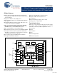
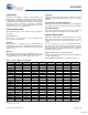
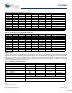
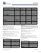
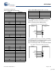
Table Of Contents
- EZ-Host Features
- Typical Applications
- Introduction
- Functional Overview
- Interface Descriptions
- USB Interface
- OTG Interface
- External Memory Interface
- General Purpose IO Interface (GPIO)
- UART Interface
- I2C EEPROM Interface
- Serial Peripheral Interface
- High-Speed Serial Interface
- Programmable Pulse/PWM Interface
- Host Port Interface
- IDE Interface
- Charge Pump Interface
- Booster Interface
- Crystal Interface
- Boot Configuration Interface
- Operational Modes
- Power Savings and Reset Description
- Memory Map
- Registers
- Processor Control Registers
- CPU Flags Register [0xC000] [R]
- Bank Register [0xC002] [R/W]
- Hardware Revision Register [0xC004] [R]
- CPU Speed Register [0xC008] [R/W]
- Power Control Register [0xC00A] [R/W]
- Interrupt Enable Register [0xC00E] [R/W]
- Breakpoint Register [0xC014] [R/W]
- USB Diagnostic Register [0xC03C] [R/W]
- Memory Diagnostic Register [0xC03E] [W]
- External Memory Registers
- Timer Registers
- General USB Registers
- USB Host Only Registers
- Host n Control Register [R/W]
- Host n Address Register [R/W]
- Host n Count Register [R/W]
- Host n Endpoint Status Register [R]
- Host n PID Register [W]
- Host n Count Result Register [R]
- Host n Device Address Register [W]
- Host n Interrupt Enable Register [R/W]
- Host n Status Register [R/W]
- Host n SOF/EOP Count Register [R/W]
- Host n SOF/EOP Counter Register [R]
- Host n Frame Register [R]
- USB Device Only Registers
- Device n Endpoint n Control Register [R/W]
- Device n Endpoint n Address Register [R/W]
- Device n Endpoint n Count Register [R/W]
- Device n Endpoint n Status Register [R/W]
- Device n Endpoint n Count Result Register [R/W]
- Device n Port Select Register [R/W]
- Device n Interrupt Enable Register [R/W]
- Device n Address Register [W]
- Device n Status Register [R/W]
- Device n Frame Number Register [R]
- Device n SOF/EOP Count Register [W]
- OTG Control Registers
- GPIO Registers
- IDE Registers
- HSS Registers
- HSS Control Register [0xC070] [R/W]
- HSS Baud Rate Register [0xC072] [R/W]
- HSS Transmit Gap Register [0xC074] [R/W]
- HSS Data Register [0xC076] [R/W]
- HSS Receive Address Register [0xC078] [R/W]
- HSS Receive Counter Register [0xC07A] [R/W]
- HSS Transmit Address Register [0xC07C] [R/W]
- HSS Transmit Counter Register [0xC07E] [R/W]
- HPI Registers
- SPI Registers
- SPI Configuration Register [0xC0C8] [R/W]
- SPI Control Register [0xC0CA] [R/W]
- SPI Interrupt Enable Register [0xC0CC] [R/W]
- SPI Status Register [0xC0CE] [R]
- SPI Interrupt Clear Register [0xC0D0] [W]
- SPI CRC Control Register [0xC0D2] [R/W]
- SPI CRC Value Register [0xC0D4] [R/W]
- SPI Data Register [0xC0D6] [R/W]
- SPI Transmit Address Register [0xC0D8] [R/W]
- SPI Transmit Count Register [0xC0DA] [R/W]
- SPI Receive Address Register [0xC0DC [R/W]
- SPI Receive Count Register [0xC0DE] [R/W]
- UART Registers
- PWM Registers
- Processor Control Registers
- Pin Diagram
- Pin Descriptions
- Absolute Maximum Ratings
- Operating Conditions
- Crystal Requirements (XTALIN, XTALOUT)
- DC Characteristics
- AC Timing Characteristics
- Register Summary
- Ordering Information
- Package Diagrams
- Document History Page
- Sales, Solutions, and Legal Information
CY7C67300
Document #: 38-08015 Rev. *J Page 8 of 99
SPI Pins
The SPI port has a few different pin location options as shown in
Table 9. The port location is selectable via the GPIO control
register [0xC006].
High-Speed Serial Interface
EZ-Host provides an HSS interface. The HSS interface is a
programmable serial connection with baud rate from 9600 baud
to 2.0M baud. The HSS interface supports both byte and block
mode operations and also hardware and software handshaking.
Complete control of EZ-Host can be accomplished through this
interface via an extensible API and communication protocol. The
HSS interface can be exposed through GPIO pins or the External
Memory port.
HSS Features
■ 8 bits, no parity code
■ Programmable baud rate from 9600 baud to 2M baud
■ Selectable 1- or 2-stop bit on transmit
■ Programmable inter-character gap timing for Block Transmit
■ 8-byte receive FIFO
■ Glitch filter on receive
■ Block mode transfer directly to/from EZ-Host internal memory
(DMA transfer)
■ Selectable CTS/RTS hardware signal handshake protocol
■ Selectable XON/XOFF software handshake protocol
■ Programmable Receive interrupt, Block Transfer Done inter-
rupts
■ Complete access to internal memory
HSS Pins
The HSS port has a few different pin location options as shown
in Table 10. The port location is selectable via the GPIO control
register [0xC006].
Programmable Pulse/PWM Interface
EZ-Host has four built in PWM output channels. Each channel
provides a programmable timing generator sequence that can be
used to interface to various image sensors or other applications.
The PWM interface is exposed through GPIO pins.
Programmable Pulse/PWM Features
■ Four independent programmable waveform generators
■ Programmable predefined frequencies ranging from 5.90 KHz
to 48 MHz
■ Configurable polarity
■ Continuous and one-shot mode available
Programmable Pulse/PWM Pins.
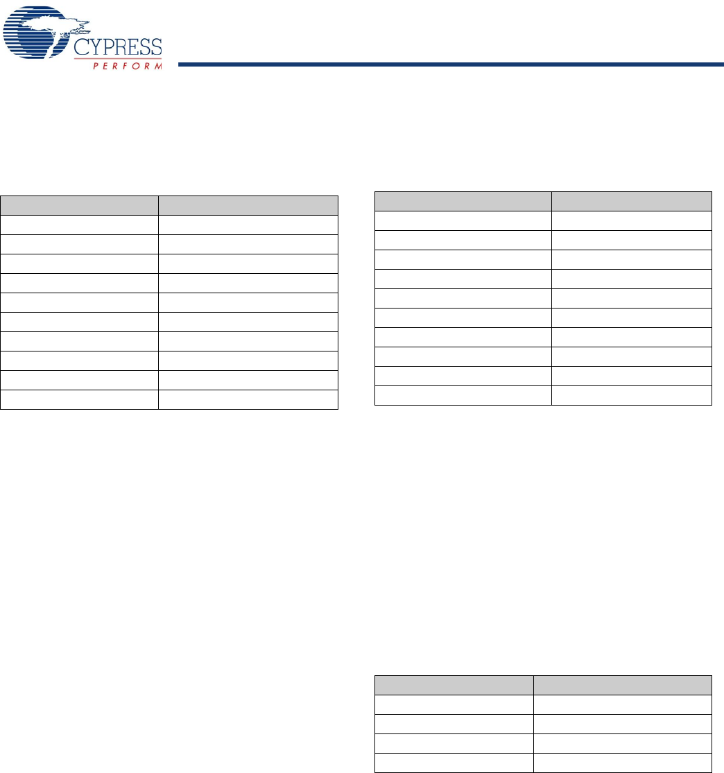
Table 9. SPI Interface Pins
Pin Name Pin Number
Default Location
nSSI 56 or 65
SCK 61
MOSI 60
MISO 66
Alternate Location
nSSI 73
SCK 72
MOSI 71
MISO 74
Table 10. HSS Interface Pins
Pin Name Pin Number
Default Location
CTS 44
RTS 53
RXD 54
TXD 55
Alternate Location
CTS 67
RTS 68
RXD 69
TXD 70
Table 11. PWM Interface Pins
Pin Name Pin Number
PWM3 44
PWM2 53
PWM1 54
PWM0 55
[+] Feedback