
Programmable Embedded USB Host and Peripheral Controller with Automotive AEC Grade Support Specification Sheet
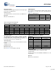
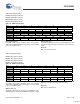
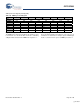
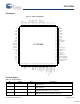
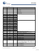
Table Of Contents
- EZ-Host Features
- Typical Applications
- Introduction
- Functional Overview
- Interface Descriptions
- USB Interface
- OTG Interface
- External Memory Interface
- General Purpose IO Interface (GPIO)
- UART Interface
- I2C EEPROM Interface
- Serial Peripheral Interface
- High-Speed Serial Interface
- Programmable Pulse/PWM Interface
- Host Port Interface
- IDE Interface
- Charge Pump Interface
- Booster Interface
- Crystal Interface
- Boot Configuration Interface
- Operational Modes
- Power Savings and Reset Description
- Memory Map
- Registers
- Processor Control Registers
- CPU Flags Register [0xC000] [R]
- Bank Register [0xC002] [R/W]
- Hardware Revision Register [0xC004] [R]
- CPU Speed Register [0xC008] [R/W]
- Power Control Register [0xC00A] [R/W]
- Interrupt Enable Register [0xC00E] [R/W]
- Breakpoint Register [0xC014] [R/W]
- USB Diagnostic Register [0xC03C] [R/W]
- Memory Diagnostic Register [0xC03E] [W]
- External Memory Registers
- Timer Registers
- General USB Registers
- USB Host Only Registers
- Host n Control Register [R/W]
- Host n Address Register [R/W]
- Host n Count Register [R/W]
- Host n Endpoint Status Register [R]
- Host n PID Register [W]
- Host n Count Result Register [R]
- Host n Device Address Register [W]
- Host n Interrupt Enable Register [R/W]
- Host n Status Register [R/W]
- Host n SOF/EOP Count Register [R/W]
- Host n SOF/EOP Counter Register [R]
- Host n Frame Register [R]
- USB Device Only Registers
- Device n Endpoint n Control Register [R/W]
- Device n Endpoint n Address Register [R/W]
- Device n Endpoint n Count Register [R/W]
- Device n Endpoint n Status Register [R/W]
- Device n Endpoint n Count Result Register [R/W]
- Device n Port Select Register [R/W]
- Device n Interrupt Enable Register [R/W]
- Device n Address Register [W]
- Device n Status Register [R/W]
- Device n Frame Number Register [R]
- Device n SOF/EOP Count Register [W]
- OTG Control Registers
- GPIO Registers
- IDE Registers
- HSS Registers
- HSS Control Register [0xC070] [R/W]
- HSS Baud Rate Register [0xC072] [R/W]
- HSS Transmit Gap Register [0xC074] [R/W]
- HSS Data Register [0xC076] [R/W]
- HSS Receive Address Register [0xC078] [R/W]
- HSS Receive Counter Register [0xC07A] [R/W]
- HSS Transmit Address Register [0xC07C] [R/W]
- HSS Transmit Counter Register [0xC07E] [R/W]
- HPI Registers
- SPI Registers
- SPI Configuration Register [0xC0C8] [R/W]
- SPI Control Register [0xC0CA] [R/W]
- SPI Interrupt Enable Register [0xC0CC] [R/W]
- SPI Status Register [0xC0CE] [R]
- SPI Interrupt Clear Register [0xC0D0] [W]
- SPI CRC Control Register [0xC0D2] [R/W]
- SPI CRC Value Register [0xC0D4] [R/W]
- SPI Data Register [0xC0D6] [R/W]
- SPI Transmit Address Register [0xC0D8] [R/W]
- SPI Transmit Count Register [0xC0DA] [R/W]
- SPI Receive Address Register [0xC0DC [R/W]
- SPI Receive Count Register [0xC0DE] [R/W]
- UART Registers
- PWM Registers
- Processor Control Registers
- Pin Diagram
- Pin Descriptions
- Absolute Maximum Ratings
- Operating Conditions
- Crystal Requirements (XTALIN, XTALOUT)
- DC Characteristics
- AC Timing Characteristics
- Register Summary
- Ordering Information
- Package Diagrams
- Document History Page
- Sales, Solutions, and Legal Information
CY7C67300
Document #: 38-08015 Rev. *J Page 79 of 99
Pin Diagram
Pin Descriptions
26
27 28 29 30
31
32 33 34 35 36 37 38 39 40 41 42 43 44 45 46 47 48 49 50
GPIO24/INT/IORDY/IRQ0
GND
A10
XTALOUT
XTALIN
A11
A12
A13
A14
nXMEMSEL
nXROMSEL
nXRAMSEL
VCC
A15/CLKSEL
GPIO31/SCL
GPIO30/SDA
GPIO29/OTGID
GPIO28/TX
GPIO27/RX
GPIO26/CTS/PWM3
GPIO25/IRQ1
GPIO23/nRD/IOR
GPIO22/nWR/IOW
GPIO21/nCS
GPIO20/A1/CS1
A9
A8
DP1A
DM1A
AVCC
A7
DP1B
DM1B
A6
BOOSTVCC
BOOSTGND
VSWITCH
CSWITCHA
CSWITCHB
OTGVBUS
DP2A
DM2A
A5
A4
AGND
DP2B
DM2B
A3
A2
A1
25
24
23
22
21
20
19
18
17
16
15
14
13
12
11
10
9
8
7
6
5
4
3
2
1
100
99 98 97 96
95
94 93 92 91 90 89 88 87 86 85 84 83 82 81 80 79 78 77 76
GND
nBEL/A0
nBEH
A16
A17
A18
GPIO0/D0
GPIO1/D1
GPIO2/D2
GPIO3/D3
GPIO4/D4
GPIO5/D5
VCC
GPIO6/D6
GPIO7/D7
nRESET
Reserved
D0
D1
D2
D4
D5
D6
D7
D3
GND
GPIO19/A0/CS0
GPIO18/A2/RTS/PWM2
GPIO17/A1/RXD/PWM1
GPIO16/A0/TXD/PWM0
GPIO15/D15/nSSI
GPIO14/D14
GPIO13/D13
GPIO12/D12
GPIO11/D11/MOSI
GPIO10/D10/SCK
nRD
VCC
nWR
GPIO9/D9/nSSI
GPIO8/D8/MISO
D15/CTS
D14/RTS
D13/RXD
D12/TXD
D11/MOSI
D10/SCK
D9/nSSI
D8/MISO
GND
52
53
54
55
56
57
58
59
60
61
62
63
64
65
66
67
68
69
70
71
72
73
74
75
51
CY7C67300
Figure 11. EZ-Host Pin Diagram
Table 131. Pin Descriptions
Pin Name Type Description
67 D15/CTS IO D15: External Memory Data Bus
CTS: HSS CTS
68 D14/RTS IO
D14: External Memory Data Bus
RTS: HSS RTS
69 D13/RXD IO
D13: External Memory Data Bus
RXD: HSS RXD (Data is received on this pin)
70 D12/TXD IO
D12: External Memory Data Bus
TXD: HSS TXD (Data is transmitted from this pin)
[+] Feedback