
Programmable Embedded USB Host and Peripheral Controller with Automotive AEC Grade Support Specification Sheet
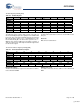
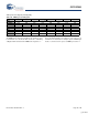
Table Of Contents
- EZ-Host Features
- Typical Applications
- Introduction
- Functional Overview
- Interface Descriptions
- USB Interface
- OTG Interface
- External Memory Interface
- General Purpose IO Interface (GPIO)
- UART Interface
- I2C EEPROM Interface
- Serial Peripheral Interface
- High-Speed Serial Interface
- Programmable Pulse/PWM Interface
- Host Port Interface
- IDE Interface
- Charge Pump Interface
- Booster Interface
- Crystal Interface
- Boot Configuration Interface
- Operational Modes
- Power Savings and Reset Description
- Memory Map
- Registers
- Processor Control Registers
- CPU Flags Register [0xC000] [R]
- Bank Register [0xC002] [R/W]
- Hardware Revision Register [0xC004] [R]
- CPU Speed Register [0xC008] [R/W]
- Power Control Register [0xC00A] [R/W]
- Interrupt Enable Register [0xC00E] [R/W]
- Breakpoint Register [0xC014] [R/W]
- USB Diagnostic Register [0xC03C] [R/W]
- Memory Diagnostic Register [0xC03E] [W]
- External Memory Registers
- Timer Registers
- General USB Registers
- USB Host Only Registers
- Host n Control Register [R/W]
- Host n Address Register [R/W]
- Host n Count Register [R/W]
- Host n Endpoint Status Register [R]
- Host n PID Register [W]
- Host n Count Result Register [R]
- Host n Device Address Register [W]
- Host n Interrupt Enable Register [R/W]
- Host n Status Register [R/W]
- Host n SOF/EOP Count Register [R/W]
- Host n SOF/EOP Counter Register [R]
- Host n Frame Register [R]
- USB Device Only Registers
- Device n Endpoint n Control Register [R/W]
- Device n Endpoint n Address Register [R/W]
- Device n Endpoint n Count Register [R/W]
- Device n Endpoint n Status Register [R/W]
- Device n Endpoint n Count Result Register [R/W]
- Device n Port Select Register [R/W]
- Device n Interrupt Enable Register [R/W]
- Device n Address Register [W]
- Device n Status Register [R/W]
- Device n Frame Number Register [R]
- Device n SOF/EOP Count Register [W]
- OTG Control Registers
- GPIO Registers
- IDE Registers
- HSS Registers
- HSS Control Register [0xC070] [R/W]
- HSS Baud Rate Register [0xC072] [R/W]
- HSS Transmit Gap Register [0xC074] [R/W]
- HSS Data Register [0xC076] [R/W]
- HSS Receive Address Register [0xC078] [R/W]
- HSS Receive Counter Register [0xC07A] [R/W]
- HSS Transmit Address Register [0xC07C] [R/W]
- HSS Transmit Counter Register [0xC07E] [R/W]
- HPI Registers
- SPI Registers
- SPI Configuration Register [0xC0C8] [R/W]
- SPI Control Register [0xC0CA] [R/W]
- SPI Interrupt Enable Register [0xC0CC] [R/W]
- SPI Status Register [0xC0CE] [R]
- SPI Interrupt Clear Register [0xC0D0] [W]
- SPI CRC Control Register [0xC0D2] [R/W]
- SPI CRC Value Register [0xC0D4] [R/W]
- SPI Data Register [0xC0D6] [R/W]
- SPI Transmit Address Register [0xC0D8] [R/W]
- SPI Transmit Count Register [0xC0DA] [R/W]
- SPI Receive Address Register [0xC0DC [R/W]
- SPI Receive Count Register [0xC0DE] [R/W]
- UART Registers
- PWM Registers
- Processor Control Registers
- Pin Diagram
- Pin Descriptions
- Absolute Maximum Ratings
- Operating Conditions
- Crystal Requirements (XTALIN, XTALOUT)
- DC Characteristics
- AC Timing Characteristics
- Register Summary
- Ordering Information
- Package Diagrams
- Document History Page
- Sales, Solutions, and Legal Information
CY7C67300
Document #: 38-08015 Rev. *J Page 76 of 99
Mode Select (Bit 8)
The Mode Select bit selects between continuous PWM cycling
and one shot mode. The default is continuous repeat.
1: Enable One Shot mode. The mode runs the number of counter
cycles set in the PWM Cycle Count register and then stops.
0: Enable Continuous mode. Runs in continuous mode and
starts over after the PWM cycle count is reached.
PWM 3 Polarity Select (Bit 7)
The PWM 3 Polarity Select bit selects the polarity for PWM 3.
1: Sets the polarity to active HIGH or rising edge pulse
0: Sets the polarity to active LOW
PWM 2 Polarity Select (Bit 6)
The PWM 2 Polarity Select bit selects the polarity for PWM 2.
1: Sets the polarity to active HIGH or rising edge pulse
0: Sets the polarity to active LOW
PWM 1 Polarity Select (Bit 5)
The PWM 1 Polarity Select bit selects the polarity for PWM 1.
1: Sets the polarity to active HIGH or rising edge pulse
0: Sets the polarity to active LOW
PWM 0 Polarity Select (Bit 4)
The PWM 0 Polarity Select bit selects the polarity for PWM 0.
1: Sets the polarity to active HIGH or rising edge pulse
0: Sets the polarity to active LOW
PWM 3 Enable (Bit 3)
The PWM 3 Enable bit enables or disables PWM 3.
1: Enable PWM 3
0: Disable PWM 3
PWM 2 Enable (Bit 2)
The PWM 2 Enable bit enables or disables PWM 2.
1: Enable PWM 2
0: Disable PWM 2
PWM 1 Enable (Bit 1)
The PWM 1 Enable bit enables or disables PWM 1.
1: Enable PWM 1
0: Disable PWM 1
PWM 0 Enable (Bit 0)
The PWM 0 Enable bit enables or disables PWM 0.
1: Enable PWM 0
0: Disable PWM 0
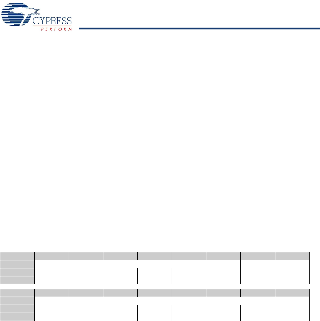
PWM Maximum Count Register [0xC0E8] [R/W]
Register Description
The PWM Maximum Count register designates the maximum
window for each pulse cycle. Each count tick is based on the
clock frequency set in the PWM Control register.
Count (Bits [9:0])
The Count field sets the maximum cycle time.
Reserved
Write all reserved bits with ’0’.
Table 127. PWM Maximum Count Register
Bit # 15 14 13 12 11 10 9 8
Field Reserved Count...
Read/Write - - - - - - R/W R/W
Default 0 0 0 0 0 0 0 0
Bit # 7 6 5 4 3 2 1 0
Field ...Count
Read/Write R/W R/W R/W R/W R/W R/W R/W R/W
Default 0 0 0 0 0 0 0 0
[+] Feedback