
Programmable Embedded USB Host and Peripheral Controller with Automotive AEC Grade Support Specification Sheet
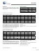
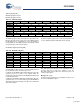
Table Of Contents
- EZ-Host Features
- Typical Applications
- Introduction
- Functional Overview
- Interface Descriptions
- USB Interface
- OTG Interface
- External Memory Interface
- General Purpose IO Interface (GPIO)
- UART Interface
- I2C EEPROM Interface
- Serial Peripheral Interface
- High-Speed Serial Interface
- Programmable Pulse/PWM Interface
- Host Port Interface
- IDE Interface
- Charge Pump Interface
- Booster Interface
- Crystal Interface
- Boot Configuration Interface
- Operational Modes
- Power Savings and Reset Description
- Memory Map
- Registers
- Processor Control Registers
- CPU Flags Register [0xC000] [R]
- Bank Register [0xC002] [R/W]
- Hardware Revision Register [0xC004] [R]
- CPU Speed Register [0xC008] [R/W]
- Power Control Register [0xC00A] [R/W]
- Interrupt Enable Register [0xC00E] [R/W]
- Breakpoint Register [0xC014] [R/W]
- USB Diagnostic Register [0xC03C] [R/W]
- Memory Diagnostic Register [0xC03E] [W]
- External Memory Registers
- Timer Registers
- General USB Registers
- USB Host Only Registers
- Host n Control Register [R/W]
- Host n Address Register [R/W]
- Host n Count Register [R/W]
- Host n Endpoint Status Register [R]
- Host n PID Register [W]
- Host n Count Result Register [R]
- Host n Device Address Register [W]
- Host n Interrupt Enable Register [R/W]
- Host n Status Register [R/W]
- Host n SOF/EOP Count Register [R/W]
- Host n SOF/EOP Counter Register [R]
- Host n Frame Register [R]
- USB Device Only Registers
- Device n Endpoint n Control Register [R/W]
- Device n Endpoint n Address Register [R/W]
- Device n Endpoint n Count Register [R/W]
- Device n Endpoint n Status Register [R/W]
- Device n Endpoint n Count Result Register [R/W]
- Device n Port Select Register [R/W]
- Device n Interrupt Enable Register [R/W]
- Device n Address Register [W]
- Device n Status Register [R/W]
- Device n Frame Number Register [R]
- Device n SOF/EOP Count Register [W]
- OTG Control Registers
- GPIO Registers
- IDE Registers
- HSS Registers
- HSS Control Register [0xC070] [R/W]
- HSS Baud Rate Register [0xC072] [R/W]
- HSS Transmit Gap Register [0xC074] [R/W]
- HSS Data Register [0xC076] [R/W]
- HSS Receive Address Register [0xC078] [R/W]
- HSS Receive Counter Register [0xC07A] [R/W]
- HSS Transmit Address Register [0xC07C] [R/W]
- HSS Transmit Counter Register [0xC07E] [R/W]
- HPI Registers
- SPI Registers
- SPI Configuration Register [0xC0C8] [R/W]
- SPI Control Register [0xC0CA] [R/W]
- SPI Interrupt Enable Register [0xC0CC] [R/W]
- SPI Status Register [0xC0CE] [R]
- SPI Interrupt Clear Register [0xC0D0] [W]
- SPI CRC Control Register [0xC0D2] [R/W]
- SPI CRC Value Register [0xC0D4] [R/W]
- SPI Data Register [0xC0D6] [R/W]
- SPI Transmit Address Register [0xC0D8] [R/W]
- SPI Transmit Count Register [0xC0DA] [R/W]
- SPI Receive Address Register [0xC0DC [R/W]
- SPI Receive Count Register [0xC0DE] [R/W]
- UART Registers
- PWM Registers
- Processor Control Registers
- Pin Diagram
- Pin Descriptions
- Absolute Maximum Ratings
- Operating Conditions
- Crystal Requirements (XTALIN, XTALOUT)
- DC Characteristics
- AC Timing Characteristics
- Register Summary
- Ordering Information
- Package Diagrams
- Document History Page
- Sales, Solutions, and Legal Information
CY7C67300
Document #: 38-08015 Rev. *J Page 70 of 99
CRC Enable (Bit 13)
The CRC Enable bit enables or disables the CRC operation.
1: Enables CRC operation
0: Disables CRC operation
CRC Clear (Bit 12)
The CRC Clear bit clears the CRC with a load of all ones. This
bit is self clearing and always reads ‘0’.
1: Clear CRC with all ones
0: No Function
Receive CRC (Bit 11)
The Receive CRC bit determines whether the receive bit stream
or the transmit bit stream is used for the CRC data input in full
duplex mode. This bit is a don’t care in half duplex mode.
1: Assigns the receive bit stream
0: Assigns the transmit bit stream
One in CRC (Bit 10)
The One in CRC bit is a read only bit that indicates if the CRC
value is all zeros or not
1: CRC value is not all zeros
0: CRC value is all zeros
Zero in CRC (Bit 9)
The Zero in CRC bit is a read only bit that indicates if the CRC
value is all ones or not.
1: CRC value is not all ones
0: CRC value is all ones
Reserved
Write all reserved bits with ’0’.
SPI CRC Value Register [0xC0D4] [R/W]
Register Description
The SPI CRC Value register contains the CRC value.
CRC (Bits [15:0])
The CRC field contains the SPI CRC. In CRC Mode CRC7, the
CRC value is a seven bit value [6:0]. Therefore, bits [15:7] are
invalid in CRC7 mode.
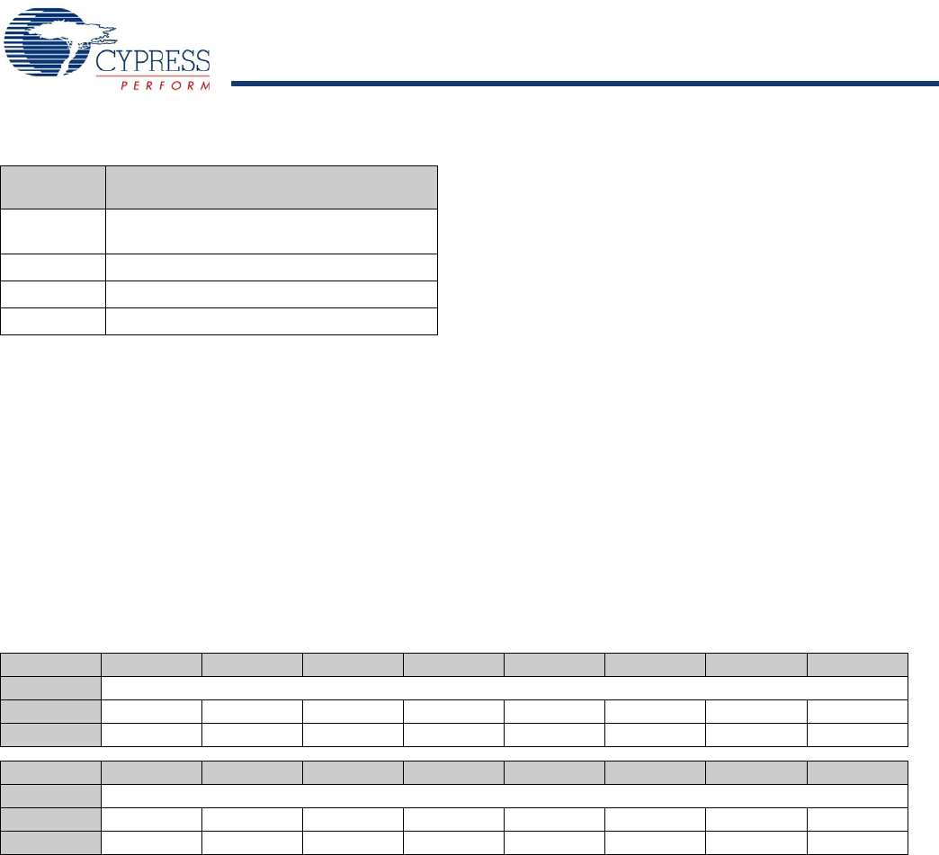
Table 112. CRC Mode Definition
CRCMode
[15:14]
CRC Polynomial
00 MMC 16 bit: X^16 + X^12 + X^5 + 1(CCITT
Standard)
01 CRC7 7 bit: X^7+ X^3 + 1
10 MST 16 bit: X^16+ X^15 + X^2 + 1
11 Reserved, 16 bit polynomial 1
Table 113. SPI CRC Value Register
Bit # 15 14 13 12 11 10 9 8
Field CRC...
Read/Write R/W R/W R/W R/W R/W R/W R/W R/W
Default 1 1 1 1 1 1 1 1
Bit # 7 6 5 4 3 2 1 0
Field ...CRC
Read/Write R/W R/W R/W R/W R/W R/W R/W R/W
Default 1 1 1 1 1 1 1 1
[+] Feedback