
Programmable Embedded USB Host and Peripheral Controller with Automotive AEC Grade Support Specification Sheet
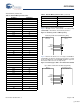
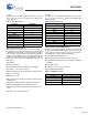
Table Of Contents
- EZ-Host Features
- Typical Applications
- Introduction
- Functional Overview
- Interface Descriptions
- USB Interface
- OTG Interface
- External Memory Interface
- General Purpose IO Interface (GPIO)
- UART Interface
- I2C EEPROM Interface
- Serial Peripheral Interface
- High-Speed Serial Interface
- Programmable Pulse/PWM Interface
- Host Port Interface
- IDE Interface
- Charge Pump Interface
- Booster Interface
- Crystal Interface
- Boot Configuration Interface
- Operational Modes
- Power Savings and Reset Description
- Memory Map
- Registers
- Processor Control Registers
- CPU Flags Register [0xC000] [R]
- Bank Register [0xC002] [R/W]
- Hardware Revision Register [0xC004] [R]
- CPU Speed Register [0xC008] [R/W]
- Power Control Register [0xC00A] [R/W]
- Interrupt Enable Register [0xC00E] [R/W]
- Breakpoint Register [0xC014] [R/W]
- USB Diagnostic Register [0xC03C] [R/W]
- Memory Diagnostic Register [0xC03E] [W]
- External Memory Registers
- Timer Registers
- General USB Registers
- USB Host Only Registers
- Host n Control Register [R/W]
- Host n Address Register [R/W]
- Host n Count Register [R/W]
- Host n Endpoint Status Register [R]
- Host n PID Register [W]
- Host n Count Result Register [R]
- Host n Device Address Register [W]
- Host n Interrupt Enable Register [R/W]
- Host n Status Register [R/W]
- Host n SOF/EOP Count Register [R/W]
- Host n SOF/EOP Counter Register [R]
- Host n Frame Register [R]
- USB Device Only Registers
- Device n Endpoint n Control Register [R/W]
- Device n Endpoint n Address Register [R/W]
- Device n Endpoint n Count Register [R/W]
- Device n Endpoint n Status Register [R/W]
- Device n Endpoint n Count Result Register [R/W]
- Device n Port Select Register [R/W]
- Device n Interrupt Enable Register [R/W]
- Device n Address Register [W]
- Device n Status Register [R/W]
- Device n Frame Number Register [R]
- Device n SOF/EOP Count Register [W]
- OTG Control Registers
- GPIO Registers
- IDE Registers
- HSS Registers
- HSS Control Register [0xC070] [R/W]
- HSS Baud Rate Register [0xC072] [R/W]
- HSS Transmit Gap Register [0xC074] [R/W]
- HSS Data Register [0xC076] [R/W]
- HSS Receive Address Register [0xC078] [R/W]
- HSS Receive Counter Register [0xC07A] [R/W]
- HSS Transmit Address Register [0xC07C] [R/W]
- HSS Transmit Counter Register [0xC07E] [R/W]
- HPI Registers
- SPI Registers
- SPI Configuration Register [0xC0C8] [R/W]
- SPI Control Register [0xC0CA] [R/W]
- SPI Interrupt Enable Register [0xC0CC] [R/W]
- SPI Status Register [0xC0CE] [R]
- SPI Interrupt Clear Register [0xC0D0] [W]
- SPI CRC Control Register [0xC0D2] [R/W]
- SPI CRC Value Register [0xC0D4] [R/W]
- SPI Data Register [0xC0D6] [R/W]
- SPI Transmit Address Register [0xC0D8] [R/W]
- SPI Transmit Count Register [0xC0DA] [R/W]
- SPI Receive Address Register [0xC0DC [R/W]
- SPI Receive Count Register [0xC0DE] [R/W]
- UART Registers
- PWM Registers
- Processor Control Registers
- Pin Diagram
- Pin Descriptions
- Absolute Maximum Ratings
- Operating Conditions
- Crystal Requirements (XTALIN, XTALOUT)
- DC Characteristics
- AC Timing Characteristics
- Register Summary
- Ordering Information
- Package Diagrams
- Document History Page
- Sales, Solutions, and Legal Information
CY7C67300
Document #: 38-08015 Rev. *J Page 7 of 99
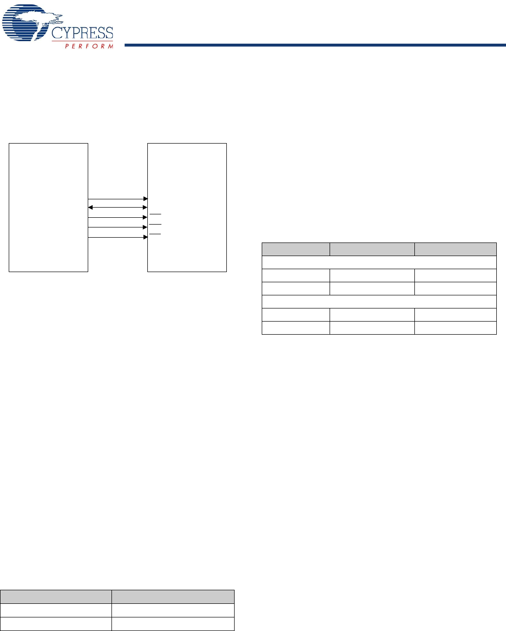
Figure 4 illustrates the interface for connecting an 8-bit ROM or
8-bit RAM to the EZ-Host external memory interface. In 8-bit
mode, up to 512K bytes of external ROM or RAM are supported.
General Purpose IO Interface (GPIO)
EZ-Host has up to 32 GPIO signals available. Several other
optional interfaces use GPIO pins as well and may reduce the
overall number of available GPIOs.
GPIO Description
All Inputs are sampled asynchronously with state changes
occurring at a rate of up to two 48 MHz clock cycles. GPIO pins
are latched directly into registers, a single flip-flop.
Unused Pin Descriptions
Ensure to tristate unused USB pins with the D+ line pulled high
through the internal pull up resistor and the D– line pulled low
through the internal pull down resistor.
Configure unused GPIO pins as outputs so they are driven low.
UART Interface
EZ-Host has a built in UART interface. The UART interface
supports data rates from 900 to 115.2K baud. It can be used as
a development port or for other interface requirements. The
UART interface is exposed through GPIO pins.
UART Features
■ Supports baud rates of 900 to 115.2K
■ 8-N-1
UART Pins.
I
2
C EEPROM Interface
EZ-Host provides a master-only I
2
C interface for external serial
EEPROMs. The serial EEPROM can be used to store application
specific code and data. Use the I
2
C interface for loading code out
of EEPROM, it is not a general I
2
C interface. The I
2
C EEPROM
interface is a BIOS implementation and is exposed through
GPIO pins. Refer to the BIOS documentation for additional
details on this interface.
I
2
C EEPROM Features
■ Supports EEPROMs up to 64 KB (512K bit)
■ Auto-detection of EEPROM size
I
2
C EEPROM Pins
Serial Peripheral Interface
EZ-Host provides a SPI interface for added connectivity. EZ-Host
may be configured as either an SPI master or SPI slave. The SPI
interface can be exposed through GPIO pins or the External
Memory port.
SPI Features
■ Master or slave mode operation
■ DMA block transfer and PIO byte transfer modes
■ Full duplex or half duplex data communication
■ 8-byte receive FIFO and 8-byte transmit FIFO
■ Selectable master SPI clock rates from 250 kHz to 12 MHz
■ Selectable master SPI clock phase and polarity
■ Slave SPI signaling synchronization and filtering
■ Slave SPI clock rates up to 2 MHz
■ Maskable interrupts for block and byte transfer modes
■ Individual bit transfer for non-byte aligned serial communi-
cation in PIO mode
■ Programmable delay timing for the active/inactive master SPI
clock
■ Auto or manual control for master mode slave select signal
■ Complete access to internal memory
Figure 4. Interfacing up to 512k × 8 for External Code/Data
Table 7. UART Interface Pins
Pin Name Pin Number
TX 42
RX 43
EZ-Host
CY7C67300
External Memory Array
Up to 512k x8
A[18:0]
nWR
nRD
nXMEMSEL
A[18:0]
WE
OE
CE
D[7:0] D[7:0]
Up to 512k x 8 External Code/Data (Page Mode)
Table 8. I
2
C EEPROM Interface Pins
Pin Name Pin Number GPIO Number
SMALL EEPROM
SCK 39 GPIO31
SDA 40 GPIO30
LARGE EEPROM
SCK 40 GPIO30
SDA 39 GPIO31
[+] Feedback