
Programmable Embedded USB Host and Peripheral Controller with Automotive AEC Grade Support Specification Sheet
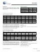
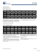
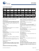
Table Of Contents
- EZ-Host Features
- Typical Applications
- Introduction
- Functional Overview
- Interface Descriptions
- USB Interface
- OTG Interface
- External Memory Interface
- General Purpose IO Interface (GPIO)
- UART Interface
- I2C EEPROM Interface
- Serial Peripheral Interface
- High-Speed Serial Interface
- Programmable Pulse/PWM Interface
- Host Port Interface
- IDE Interface
- Charge Pump Interface
- Booster Interface
- Crystal Interface
- Boot Configuration Interface
- Operational Modes
- Power Savings and Reset Description
- Memory Map
- Registers
- Processor Control Registers
- CPU Flags Register [0xC000] [R]
- Bank Register [0xC002] [R/W]
- Hardware Revision Register [0xC004] [R]
- CPU Speed Register [0xC008] [R/W]
- Power Control Register [0xC00A] [R/W]
- Interrupt Enable Register [0xC00E] [R/W]
- Breakpoint Register [0xC014] [R/W]
- USB Diagnostic Register [0xC03C] [R/W]
- Memory Diagnostic Register [0xC03E] [W]
- External Memory Registers
- Timer Registers
- General USB Registers
- USB Host Only Registers
- Host n Control Register [R/W]
- Host n Address Register [R/W]
- Host n Count Register [R/W]
- Host n Endpoint Status Register [R]
- Host n PID Register [W]
- Host n Count Result Register [R]
- Host n Device Address Register [W]
- Host n Interrupt Enable Register [R/W]
- Host n Status Register [R/W]
- Host n SOF/EOP Count Register [R/W]
- Host n SOF/EOP Counter Register [R]
- Host n Frame Register [R]
- USB Device Only Registers
- Device n Endpoint n Control Register [R/W]
- Device n Endpoint n Address Register [R/W]
- Device n Endpoint n Count Register [R/W]
- Device n Endpoint n Status Register [R/W]
- Device n Endpoint n Count Result Register [R/W]
- Device n Port Select Register [R/W]
- Device n Interrupt Enable Register [R/W]
- Device n Address Register [W]
- Device n Status Register [R/W]
- Device n Frame Number Register [R]
- Device n SOF/EOP Count Register [W]
- OTG Control Registers
- GPIO Registers
- IDE Registers
- HSS Registers
- HSS Control Register [0xC070] [R/W]
- HSS Baud Rate Register [0xC072] [R/W]
- HSS Transmit Gap Register [0xC074] [R/W]
- HSS Data Register [0xC076] [R/W]
- HSS Receive Address Register [0xC078] [R/W]
- HSS Receive Counter Register [0xC07A] [R/W]
- HSS Transmit Address Register [0xC07C] [R/W]
- HSS Transmit Counter Register [0xC07E] [R/W]
- HPI Registers
- SPI Registers
- SPI Configuration Register [0xC0C8] [R/W]
- SPI Control Register [0xC0CA] [R/W]
- SPI Interrupt Enable Register [0xC0CC] [R/W]
- SPI Status Register [0xC0CE] [R]
- SPI Interrupt Clear Register [0xC0D0] [W]
- SPI CRC Control Register [0xC0D2] [R/W]
- SPI CRC Value Register [0xC0D4] [R/W]
- SPI Data Register [0xC0D6] [R/W]
- SPI Transmit Address Register [0xC0D8] [R/W]
- SPI Transmit Count Register [0xC0DA] [R/W]
- SPI Receive Address Register [0xC0DC [R/W]
- SPI Receive Count Register [0xC0DE] [R/W]
- UART Registers
- PWM Registers
- Processor Control Registers
- Pin Diagram
- Pin Descriptions
- Absolute Maximum Ratings
- Operating Conditions
- Crystal Requirements (XTALIN, XTALOUT)
- DC Characteristics
- AC Timing Characteristics
- Register Summary
- Ordering Information
- Package Diagrams
- Document History Page
- Sales, Solutions, and Legal Information

CY7C67300
Document #: 38-08015 Rev. *J Page 67 of 99
SPI Control Register [0xC0CA] [R/W]
Register Description
The SPI Control register controls the SPI port. Fields apply to
both master and slave mode unless otherwise noted.
SCK Strobe (Bit 15)
The SCK Strobe bit starts the SCK strobe at the selected
frequency and polarity (set in the SPI Configuration register), but
not phase. This bit feature can only be enabled when in master
mode and must be during a period of inactivity. This bit is self
clearing.
1: SCK Strobe Enable
0: No Function
FIFO Init (Bit 14)
The FIFO Init bit initializes the FIFO and clears the FIFO Error
Status bit. This bit is self clearing.
1: FIFO Init Enable
0: No Function
Byte Mode (Bit 13)
The Byte Mode bit selects between PIO (byte mode) and DMA
(block mode) operation.
1: Set PIO (byte mode) operation
0: Set DMA (block mode) operation
Full Duplex (Bit 12)
The Full Duplex bit selects between full duplex and half duplex
operation.
1: Enable full duplex. Full duplex is not allowed and does not set
if the 3Wire Enable bit of the SPI Configuration register is set to
‘1’
0: Enable half duplex operation
SS Manual (Bit 11)
The SS Manual bit activates or deactivates SS if the SS Delay
Select field of the SPI Control register is all zeros and is
configured as master interface. This field only applies to master
mode.
1: Activate SS, master drives SS line asserted LOW
0: Deactivate SS, master drives SS line deasserted HIGH
Read Enable (Bit 10)
The Read Enable bit initiates a read phase for a master mode
transfer or sets the slave to receive (in slave mode).
1: Initiates a read phase for a master transfer or sets a slave to
receive. In master mode this bit is sticky and remains set until the
read transfer begins.
0: Initiates the write phase for slave operation
Transmit Ready (Bit 9)
The Transmit Ready bit is a read only bit that indicates if the
transmit port is ready to empty and ready to be written.
1: Ready for data to be written to the port. The transmit FIFO is
not full.
0: Not ready for data to be written to the port
Receive Data Ready (Bit 8)
The Receive Data Ready bit is a read only bit that indicates if the
receive port has data ready.
1: Receive port has data ready to read
0: Receive port does not have data ready
Transmit Empty (Bit 7)
The Transmit Empty bit is a read only bit that indicates if the
transmit FIFO is empty.
1: Transmit FIFO is empty
0: Transmit FIFO is not empty
Receive Full (Bit 6)
The Receive Full bit is a read only bit that indicates if the receive
FIFO is full.
1: Receive FIFO is full
0: Receive FIFO is not full
Transmit Bit Length (Bits [5:3])
The Transmit Bit Length field controls whether a full byte or
partial byte is to be transmitted. If Transmit Bit Length is ‘000’
then a full byte is transmitted. If Transmit Bit Length is ‘001’ to
‘111’, then the value indicates the number of bits that are be
transmitted.
Table 107. SPI Control Register
Bit # 15 14 13 12 11 10 9 8
Field
SCK
Strobe
FIFO
Init
Byte
Mode
Full Duplex SS
Manual
Read
Enable
Transmit
Ready
Receive
Data
Ready
Read/Write W W R/W R/W R/W R/W R R
Default 0 0 0 0 0 0 0 1
Bit # 7 6 5 4 3 2 1 0
Field
Transmit
Empty
Receive
Full
Transmit Bit Length Receive Bit Length
Read/Write R R R/W R/W R/W R/W R/W R/W
Default 1 0 0 0 0 0 0 0
[+] Feedback