
Programmable Embedded USB Host and Peripheral Controller with Automotive AEC Grade Support Specification Sheet
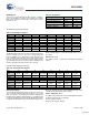
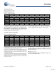
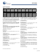
Table Of Contents
- EZ-Host Features
- Typical Applications
- Introduction
- Functional Overview
- Interface Descriptions
- USB Interface
- OTG Interface
- External Memory Interface
- General Purpose IO Interface (GPIO)
- UART Interface
- I2C EEPROM Interface
- Serial Peripheral Interface
- High-Speed Serial Interface
- Programmable Pulse/PWM Interface
- Host Port Interface
- IDE Interface
- Charge Pump Interface
- Booster Interface
- Crystal Interface
- Boot Configuration Interface
- Operational Modes
- Power Savings and Reset Description
- Memory Map
- Registers
- Processor Control Registers
- CPU Flags Register [0xC000] [R]
- Bank Register [0xC002] [R/W]
- Hardware Revision Register [0xC004] [R]
- CPU Speed Register [0xC008] [R/W]
- Power Control Register [0xC00A] [R/W]
- Interrupt Enable Register [0xC00E] [R/W]
- Breakpoint Register [0xC014] [R/W]
- USB Diagnostic Register [0xC03C] [R/W]
- Memory Diagnostic Register [0xC03E] [W]
- External Memory Registers
- Timer Registers
- General USB Registers
- USB Host Only Registers
- Host n Control Register [R/W]
- Host n Address Register [R/W]
- Host n Count Register [R/W]
- Host n Endpoint Status Register [R]
- Host n PID Register [W]
- Host n Count Result Register [R]
- Host n Device Address Register [W]
- Host n Interrupt Enable Register [R/W]
- Host n Status Register [R/W]
- Host n SOF/EOP Count Register [R/W]
- Host n SOF/EOP Counter Register [R]
- Host n Frame Register [R]
- USB Device Only Registers
- Device n Endpoint n Control Register [R/W]
- Device n Endpoint n Address Register [R/W]
- Device n Endpoint n Count Register [R/W]
- Device n Endpoint n Status Register [R/W]
- Device n Endpoint n Count Result Register [R/W]
- Device n Port Select Register [R/W]
- Device n Interrupt Enable Register [R/W]
- Device n Address Register [W]
- Device n Status Register [R/W]
- Device n Frame Number Register [R]
- Device n SOF/EOP Count Register [W]
- OTG Control Registers
- GPIO Registers
- IDE Registers
- HSS Registers
- HSS Control Register [0xC070] [R/W]
- HSS Baud Rate Register [0xC072] [R/W]
- HSS Transmit Gap Register [0xC074] [R/W]
- HSS Data Register [0xC076] [R/W]
- HSS Receive Address Register [0xC078] [R/W]
- HSS Receive Counter Register [0xC07A] [R/W]
- HSS Transmit Address Register [0xC07C] [R/W]
- HSS Transmit Counter Register [0xC07E] [R/W]
- HPI Registers
- SPI Registers
- SPI Configuration Register [0xC0C8] [R/W]
- SPI Control Register [0xC0CA] [R/W]
- SPI Interrupt Enable Register [0xC0CC] [R/W]
- SPI Status Register [0xC0CE] [R]
- SPI Interrupt Clear Register [0xC0D0] [W]
- SPI CRC Control Register [0xC0D2] [R/W]
- SPI CRC Value Register [0xC0D4] [R/W]
- SPI Data Register [0xC0D6] [R/W]
- SPI Transmit Address Register [0xC0D8] [R/W]
- SPI Transmit Count Register [0xC0DA] [R/W]
- SPI Receive Address Register [0xC0DC [R/W]
- SPI Receive Count Register [0xC0DE] [R/W]
- UART Registers
- PWM Registers
- Processor Control Registers
- Pin Diagram
- Pin Descriptions
- Absolute Maximum Ratings
- Operating Conditions
- Crystal Requirements (XTALIN, XTALOUT)
- DC Characteristics
- AC Timing Characteristics
- Register Summary
- Ordering Information
- Package Diagrams
- Document History Page
- Sales, Solutions, and Legal Information
CY7C67300
Document #: 38-08015 Rev. *J Page 61 of 99
HPI Registers
There are five registers dedicated to HPI operation. In addition,
there is an HPI status port which can be addressed over HPI.
Each of these registers is covered in this section and are summa-
rized in Table 98.
HPI Breakpoint Register [0x0140] [R]
Register Description
The HPI Breakpoint register is a special on-chip memory location
that the external processor can access using normal HPI
memory read/write cycles. This register is read only by the CPU
but is read/write by the HPI port. The contents of this register
have the same effect as the Breakpoint register [0xC014]. This
special Breakpoint register is used by software debuggers that
interface through the HPI port instead of the serial port.
When the program counter matches the Breakpoint Address, the
INT127 interrupt triggers. To clear this interrupt, write a zero a to
this register.
Address (Bits [15:0])
The Address field is a 16-bit field containing the breakpoint
address.
Interrupt Routing Register [0x0142] [R]
Register Description
The Interrupt Routing register allows the HPI port to take over
some or all of the SIE interrupts that usually go to the on-chip
CPU. This register is read only by the CPU but is read/write by
the HPI port. By setting the appropriate bit to ‘1’, the SIE interrupt
is routed to the HPI port to become the HPI_INTR signal and also
readable in the HPI Status register. The bits in this register select
where the interrupts are routed. The individual interrupt enable
is handled in the SIE interrupt enable register.
VBUS to HPI Enable (Bit 15)
The VBUS to HPI Enable bit routes the OTG VBUS interrupt to
the HPI port instead of the on-chip CPU.
1: Route signal to HPI port
0: Do not route signal to HPI port
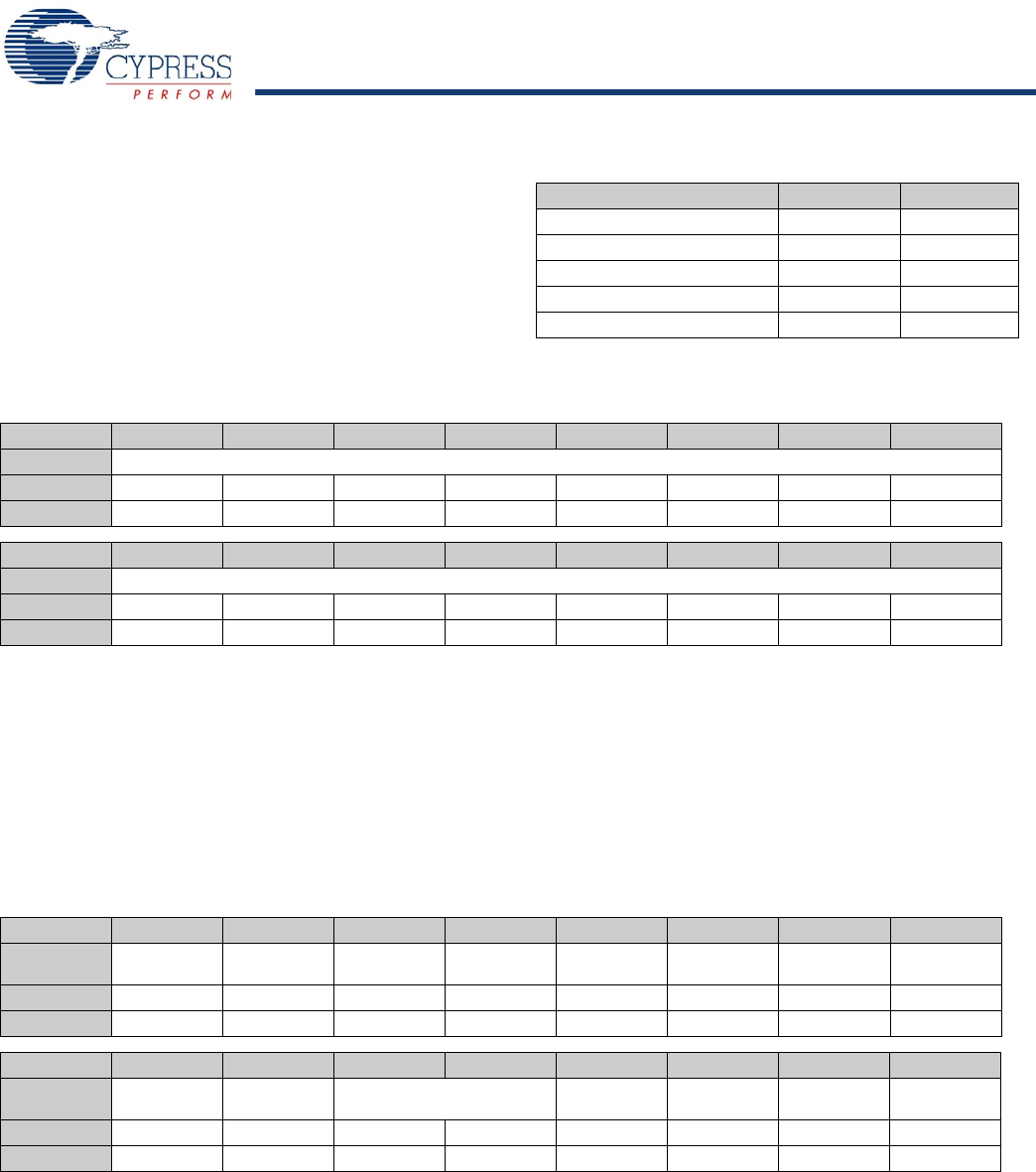
Table 98. HPI Registers
Register Name Address R/W
HPI Breakpoint Register 0x0140 R
Interrupt Routing Register 0x0142 R
SIE1msg Register 0x0144 W
SIE2msg Register 0x0148 W
HPI Mailbox Register 0xC0C6 R/W
Table 99. HPI Breakpoint Register
Bit # 15 14 13 12 11 10 9 8
Field Address...
Read/Write R R R R R R R R
Default 0 0 0 0 0 0 0 0
Bit # 7 6 5 4 3 2 1 0
Field ...Address
Read/Write R R R R R R R R
Default 0 0 0 0 0 0 0 0
Table 100. Interrupt Routing Register
Bit # 15 14 13 12 11 10 9 8
Field
VBUS to HPI
Enable
ID to HPI
Enable
SOF/EOP2 to
HPI Enable
SOF/EOP2 to
CPU Enable
SOF/EOP1 to
HPI Enable
SOF/EOP1 to
CPU Enable
Reset2 to HPI
Enable
HPI Swap 1
Enable
Read/Write - - - - - - - -
Default 0 0 0 1 0 1 0 0
Bit # 7 6 5 4 3 2 1 0
Field
Resume2 to
HPI Enable
Resume1 to
HPI Enable
Reserved Done2 to HPI
Enable
Done1 to HPI
Enable
Reset1 to HPI
Enable
HPI Swap 0
Enable
Read/Write - - - - - - - -
Default 0 0 0 0 0 0 0 0
[+] Feedback