
Programmable Embedded USB Host and Peripheral Controller with Automotive AEC Grade Support Specification Sheet
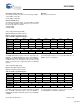
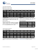
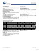
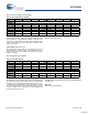
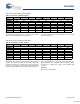
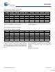
Table Of Contents
- EZ-Host Features
- Typical Applications
- Introduction
- Functional Overview
- Interface Descriptions
- USB Interface
- OTG Interface
- External Memory Interface
- General Purpose IO Interface (GPIO)
- UART Interface
- I2C EEPROM Interface
- Serial Peripheral Interface
- High-Speed Serial Interface
- Programmable Pulse/PWM Interface
- Host Port Interface
- IDE Interface
- Charge Pump Interface
- Booster Interface
- Crystal Interface
- Boot Configuration Interface
- Operational Modes
- Power Savings and Reset Description
- Memory Map
- Registers
- Processor Control Registers
- CPU Flags Register [0xC000] [R]
- Bank Register [0xC002] [R/W]
- Hardware Revision Register [0xC004] [R]
- CPU Speed Register [0xC008] [R/W]
- Power Control Register [0xC00A] [R/W]
- Interrupt Enable Register [0xC00E] [R/W]
- Breakpoint Register [0xC014] [R/W]
- USB Diagnostic Register [0xC03C] [R/W]
- Memory Diagnostic Register [0xC03E] [W]
- External Memory Registers
- Timer Registers
- General USB Registers
- USB Host Only Registers
- Host n Control Register [R/W]
- Host n Address Register [R/W]
- Host n Count Register [R/W]
- Host n Endpoint Status Register [R]
- Host n PID Register [W]
- Host n Count Result Register [R]
- Host n Device Address Register [W]
- Host n Interrupt Enable Register [R/W]
- Host n Status Register [R/W]
- Host n SOF/EOP Count Register [R/W]
- Host n SOF/EOP Counter Register [R]
- Host n Frame Register [R]
- USB Device Only Registers
- Device n Endpoint n Control Register [R/W]
- Device n Endpoint n Address Register [R/W]
- Device n Endpoint n Count Register [R/W]
- Device n Endpoint n Status Register [R/W]
- Device n Endpoint n Count Result Register [R/W]
- Device n Port Select Register [R/W]
- Device n Interrupt Enable Register [R/W]
- Device n Address Register [W]
- Device n Status Register [R/W]
- Device n Frame Number Register [R]
- Device n SOF/EOP Count Register [W]
- OTG Control Registers
- GPIO Registers
- IDE Registers
- HSS Registers
- HSS Control Register [0xC070] [R/W]
- HSS Baud Rate Register [0xC072] [R/W]
- HSS Transmit Gap Register [0xC074] [R/W]
- HSS Data Register [0xC076] [R/W]
- HSS Receive Address Register [0xC078] [R/W]
- HSS Receive Counter Register [0xC07A] [R/W]
- HSS Transmit Address Register [0xC07C] [R/W]
- HSS Transmit Counter Register [0xC07E] [R/W]
- HPI Registers
- SPI Registers
- SPI Configuration Register [0xC0C8] [R/W]
- SPI Control Register [0xC0CA] [R/W]
- SPI Interrupt Enable Register [0xC0CC] [R/W]
- SPI Status Register [0xC0CE] [R]
- SPI Interrupt Clear Register [0xC0D0] [W]
- SPI CRC Control Register [0xC0D2] [R/W]
- SPI CRC Value Register [0xC0D4] [R/W]
- SPI Data Register [0xC0D6] [R/W]
- SPI Transmit Address Register [0xC0D8] [R/W]
- SPI Transmit Count Register [0xC0DA] [R/W]
- SPI Receive Address Register [0xC0DC [R/W]
- SPI Receive Count Register [0xC0DE] [R/W]
- UART Registers
- PWM Registers
- Processor Control Registers
- Pin Diagram
- Pin Descriptions
- Absolute Maximum Ratings
- Operating Conditions
- Crystal Requirements (XTALIN, XTALOUT)
- DC Characteristics
- AC Timing Characteristics
- Register Summary
- Ordering Information
- Package Diagrams
- Document History Page
- Sales, Solutions, and Legal Information
CY7C67300
Document #: 38-08015 Rev. *J Page 60 of 99
HSS Transmit Address Register [0xC07C] [R/W]
Register Description
The HSS Transmit Address register is used as the base pointer
address for the next HSS block transmit transfer.
Address (Bits [15:0])
The Address field sets the base pointer address for the next HSS
block transmit transfer.
HSS Transmit Counter Register [0xC07E] [R/W]
Register Description
The HSS Transmit Counter register designates the block byte
length for the next HSS transmit transfer. Load this register with
the word count minus one to start the block transmit transfer. As
each byte is transmitted this register value is decremented.
When read, this register indicates the remaining length of the
transfer.
Counter (Bits [9:0])
The Counter field value is equal to the word count minus one
giving a maximum value of 0x03FF (1023) or 2048 bytes. When
the transfer is complete this register returns 0x03FF until
reloaded.
Reserved
Write all reserved bits with ’0’.
Table 96. HSS Transmit Address Register
Bit # 15 14 13 12 11 10 9 8
Field Address...
Read/Write R/W R/W R/W R/W R/W R/W R/W R/W
Default 0 0 0 0 0 0 0 0
Bit # 7 6 5 4 3 2 1 0
Field ...Address
Read/Write R/W R/W R/W R/W R/W R/W R/W R/W
Default 0 0 0 0 0 0 0 0
Table 97. HSS Transmit Counter Register
Bit # 15 14 13 12 11 10 9 8
Field Reserved Counter...
Read/Write - - - - - - R/W R/W
Default 0 0 0 0 0 0 0 0
Bit # 7 6 5 4 3 2 1 0
Field ...Counter
Read/Write R/W R/W R/W R/W R/W R/W R/W R/W
Default 0 0 0 0 0 0 0 0
[+] Feedback