
Programmable Embedded USB Host and Peripheral Controller with Automotive AEC Grade Support Specification Sheet
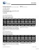
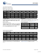
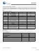
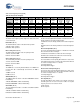
Table Of Contents
- EZ-Host Features
- Typical Applications
- Introduction
- Functional Overview
- Interface Descriptions
- USB Interface
- OTG Interface
- External Memory Interface
- General Purpose IO Interface (GPIO)
- UART Interface
- I2C EEPROM Interface
- Serial Peripheral Interface
- High-Speed Serial Interface
- Programmable Pulse/PWM Interface
- Host Port Interface
- IDE Interface
- Charge Pump Interface
- Booster Interface
- Crystal Interface
- Boot Configuration Interface
- Operational Modes
- Power Savings and Reset Description
- Memory Map
- Registers
- Processor Control Registers
- CPU Flags Register [0xC000] [R]
- Bank Register [0xC002] [R/W]
- Hardware Revision Register [0xC004] [R]
- CPU Speed Register [0xC008] [R/W]
- Power Control Register [0xC00A] [R/W]
- Interrupt Enable Register [0xC00E] [R/W]
- Breakpoint Register [0xC014] [R/W]
- USB Diagnostic Register [0xC03C] [R/W]
- Memory Diagnostic Register [0xC03E] [W]
- External Memory Registers
- Timer Registers
- General USB Registers
- USB Host Only Registers
- Host n Control Register [R/W]
- Host n Address Register [R/W]
- Host n Count Register [R/W]
- Host n Endpoint Status Register [R]
- Host n PID Register [W]
- Host n Count Result Register [R]
- Host n Device Address Register [W]
- Host n Interrupt Enable Register [R/W]
- Host n Status Register [R/W]
- Host n SOF/EOP Count Register [R/W]
- Host n SOF/EOP Counter Register [R]
- Host n Frame Register [R]
- USB Device Only Registers
- Device n Endpoint n Control Register [R/W]
- Device n Endpoint n Address Register [R/W]
- Device n Endpoint n Count Register [R/W]
- Device n Endpoint n Status Register [R/W]
- Device n Endpoint n Count Result Register [R/W]
- Device n Port Select Register [R/W]
- Device n Interrupt Enable Register [R/W]
- Device n Address Register [W]
- Device n Status Register [R/W]
- Device n Frame Number Register [R]
- Device n SOF/EOP Count Register [W]
- OTG Control Registers
- GPIO Registers
- IDE Registers
- HSS Registers
- HSS Control Register [0xC070] [R/W]
- HSS Baud Rate Register [0xC072] [R/W]
- HSS Transmit Gap Register [0xC074] [R/W]
- HSS Data Register [0xC076] [R/W]
- HSS Receive Address Register [0xC078] [R/W]
- HSS Receive Counter Register [0xC07A] [R/W]
- HSS Transmit Address Register [0xC07C] [R/W]
- HSS Transmit Counter Register [0xC07E] [R/W]
- HPI Registers
- SPI Registers
- SPI Configuration Register [0xC0C8] [R/W]
- SPI Control Register [0xC0CA] [R/W]
- SPI Interrupt Enable Register [0xC0CC] [R/W]
- SPI Status Register [0xC0CE] [R]
- SPI Interrupt Clear Register [0xC0D0] [W]
- SPI CRC Control Register [0xC0D2] [R/W]
- SPI CRC Value Register [0xC0D4] [R/W]
- SPI Data Register [0xC0D6] [R/W]
- SPI Transmit Address Register [0xC0D8] [R/W]
- SPI Transmit Count Register [0xC0DA] [R/W]
- SPI Receive Address Register [0xC0DC [R/W]
- SPI Receive Count Register [0xC0DE] [R/W]
- UART Registers
- PWM Registers
- Processor Control Registers
- Pin Diagram
- Pin Descriptions
- Absolute Maximum Ratings
- Operating Conditions
- Crystal Requirements (XTALIN, XTALOUT)
- DC Characteristics
- AC Timing Characteristics
- Register Summary
- Ordering Information
- Package Diagrams
- Document History Page
- Sales, Solutions, and Legal Information

CY7C67300
Document #: 38-08015 Rev. *J Page 56 of 99
HSS Control Register [0xC070] [R/W]
Register Description
The HSS Control register provides high level status and control
over the HSS port.
HSS Enable (Bit 15)
The HSS Enable bit enables or disables HSS operation.
1: Enables HSS operation
0: Disables HSS operation
RTS Polarity Select (Bit 14)
The RTS Polarity Select bit selects the polarity of RTS.
1: RTS is true when LOW
0: RTS is true when HIGH
CTS Polarity Select (Bit 13)
The CTS Polarity Select bit selects the polarity of CTS.
1: CTS is true when LOW
0: CTS is true when HIGH
XOFF (Bit 12)
The XOFF bit is a read only bit that indicates if an XOFF was
received. This bit is automatically cleared when an XON is
received.
1: XOFF received
0: XON received
XOFF Enable (Bit 11)
The XOFF Enable bit enables or disables XON/XOFF software
handshaking.
1: Enable XON/XOFF software handshaking
0: Disable XON/XOFF software handshaking
CTS Enable (Bit 10)
The CTS Enable bit enables or disables CTS/RTS hardware
handshaking.
1: Enable CTS/RTS hardware handshaking
0: Disable CTS/RTS hardware handshaking
Receive Interrupt Enable (Bit 9)
The Receive Interrupt Enable bit enables or disables the Receive
Ready and Receive Packet Ready interrupts.
1: Enable the Receive Ready and Receive Packet Ready inter-
rupts
0: Disable the Receive Ready and Receive Packet Ready inter-
rupts
Done Interrupt Enable (Bit 8)
The Done Interrupt Enable bit enables or disables the Transmit
Done and Receive Done interrupts.
1: Enable the Transmit Done and Receive Done interrupts
0: Disable the Transmit Done and Receive Done interrupts
Transmit Done Interrupt Flag (Bit 7)
The Transmit Done Interrupt Flag bit indicates the status of the
Transmit Done Interrupt. It sets when a block transmit is finished.
To clear the interrupt, write a ‘1’ to this bit.
1: Interrupt triggered
0: Interrupt did not trigger
Receive Done Interrupt Flag (Bit 6)
The Receive Done Interrupt Flag bit indicates the status of the
Receive Done Interrupt. It sets when a block transmit is finished.
To clear the interrupt, write a ‘1’ to this bit.
1: Interrupt triggered
0: Interrupt did not trigger
One Stop Bit (Bit 5)
The One Stop Bit bit selects between one and two stop bits for
transmit byte mode. In receive mode, the number of stop bits
may vary and does not need to be fixed.
1: One stop bit
0: Two stop bits
Table 90. HSS Control Register
Bit # 15 14 13 12 11 10 9 8
Field
HSS
Enable
RTS
Polarity
Select
CTS
Polarity
Select
XOFF XOFF
Enable
CTS
Enable
Receive
Interrupt
Enable
Done
Interrupt
Enable
Read/Write R/W R/W R/W R R/W R/W R/W R/W
Default 0 0 0 0 0 0 0 0
Bit # 7 6 5 4 3 2 1 0
Field
Transmit
Done Interrupt
Enable
Receive
Done Interrupt
Enable
One
Stop Bit
Transmit
Ready
Packet
Mode
Select
Receive
Overflow
Flag
Receive
Packet Ready
Flag
Receive
Ready
Flag
Read/Write R/W R/W R/W R R/W R/W R R
Default 0 0 0 0 0 0 0 0
[+] Feedback