
Programmable Embedded USB Host and Peripheral Controller with Automotive AEC Grade Support Specification Sheet
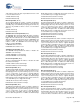
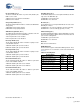
Table Of Contents
- EZ-Host Features
- Typical Applications
- Introduction
- Functional Overview
- Interface Descriptions
- USB Interface
- OTG Interface
- External Memory Interface
- General Purpose IO Interface (GPIO)
- UART Interface
- I2C EEPROM Interface
- Serial Peripheral Interface
- High-Speed Serial Interface
- Programmable Pulse/PWM Interface
- Host Port Interface
- IDE Interface
- Charge Pump Interface
- Booster Interface
- Crystal Interface
- Boot Configuration Interface
- Operational Modes
- Power Savings and Reset Description
- Memory Map
- Registers
- Processor Control Registers
- CPU Flags Register [0xC000] [R]
- Bank Register [0xC002] [R/W]
- Hardware Revision Register [0xC004] [R]
- CPU Speed Register [0xC008] [R/W]
- Power Control Register [0xC00A] [R/W]
- Interrupt Enable Register [0xC00E] [R/W]
- Breakpoint Register [0xC014] [R/W]
- USB Diagnostic Register [0xC03C] [R/W]
- Memory Diagnostic Register [0xC03E] [W]
- External Memory Registers
- Timer Registers
- General USB Registers
- USB Host Only Registers
- Host n Control Register [R/W]
- Host n Address Register [R/W]
- Host n Count Register [R/W]
- Host n Endpoint Status Register [R]
- Host n PID Register [W]
- Host n Count Result Register [R]
- Host n Device Address Register [W]
- Host n Interrupt Enable Register [R/W]
- Host n Status Register [R/W]
- Host n SOF/EOP Count Register [R/W]
- Host n SOF/EOP Counter Register [R]
- Host n Frame Register [R]
- USB Device Only Registers
- Device n Endpoint n Control Register [R/W]
- Device n Endpoint n Address Register [R/W]
- Device n Endpoint n Count Register [R/W]
- Device n Endpoint n Status Register [R/W]
- Device n Endpoint n Count Result Register [R/W]
- Device n Port Select Register [R/W]
- Device n Interrupt Enable Register [R/W]
- Device n Address Register [W]
- Device n Status Register [R/W]
- Device n Frame Number Register [R]
- Device n SOF/EOP Count Register [W]
- OTG Control Registers
- GPIO Registers
- IDE Registers
- HSS Registers
- HSS Control Register [0xC070] [R/W]
- HSS Baud Rate Register [0xC072] [R/W]
- HSS Transmit Gap Register [0xC074] [R/W]
- HSS Data Register [0xC076] [R/W]
- HSS Receive Address Register [0xC078] [R/W]
- HSS Receive Counter Register [0xC07A] [R/W]
- HSS Transmit Address Register [0xC07C] [R/W]
- HSS Transmit Counter Register [0xC07E] [R/W]
- HPI Registers
- SPI Registers
- SPI Configuration Register [0xC0C8] [R/W]
- SPI Control Register [0xC0CA] [R/W]
- SPI Interrupt Enable Register [0xC0CC] [R/W]
- SPI Status Register [0xC0CE] [R]
- SPI Interrupt Clear Register [0xC0D0] [W]
- SPI CRC Control Register [0xC0D2] [R/W]
- SPI CRC Value Register [0xC0D4] [R/W]
- SPI Data Register [0xC0D6] [R/W]
- SPI Transmit Address Register [0xC0D8] [R/W]
- SPI Transmit Count Register [0xC0DA] [R/W]
- SPI Receive Address Register [0xC0DC [R/W]
- SPI Receive Count Register [0xC0DE] [R/W]
- UART Registers
- PWM Registers
- Processor Control Registers
- Pin Diagram
- Pin Descriptions
- Absolute Maximum Ratings
- Operating Conditions
- Crystal Requirements (XTALIN, XTALOUT)
- DC Characteristics
- AC Timing Characteristics
- Register Summary
- Ordering Information
- Package Diagrams
- Document History Page
- Sales, Solutions, and Legal Information

CY7C67300
Document #: 38-08015 Rev. *J Page 50 of 99
GPIO Control Register [0xC006] [R/W]
Register Description
The GPIO Control register configures the GPIO pins for various
interface options. It also controls the polarity of the GPIO
interrupt on IRQ1 (GPIO25) and IRQ0 (GPIO24).
Write Protect Enable (Bit 15)
The Write Protect Enable bit enables or disables the GPIO write
protect. When Write Protect is enabled, the GPIO Mode Select
[15:8] field is read only until a chip reset.
1: Enable Write Protect
0: Disable Write Protect
UD (Bit 14)
The UD bit routes the Host/Device 1A Port’s transmitter enable
status to GPIO[30]. This is for use with an external ESD
protection circuit when needed.
1: Route the signal to GPIO[30]
0: Do not route the signal to GPIO[30]
SAS Enable (Bit 11)
The SAS Enable bit, when in SPI mode, reroutes the SPI port
SPI_nSSI pin to GPIO[15] rather then GPIO[9] or XD[9] (per
SG/SX).
1: Reroute SPI_nss to GPIO[30]
0: Leave SPI_nss on GPIO[9]
Mode Select (Bits [10:8])
The Mode Select field selects how GPIO[15:0] and GPIO[24:19]
are used as defined in Table 78.
HSS Enable (Bit 7)
The HSS Enable bit routes HSS to GPIO[26, 18:16]. If the HSS
XD Enable bit is set, it overrides this bit and HSS is routed to
XD[15:12].
1: HSS is routed to GPIO
0: HSS is not routed to GPIOs. GPIO[26, 18:16] are free for other
purposes
HSS XD Enable (Bit 6)
The HSS XD Enable bit routes HSS to XD[15:12] (external
memory data bus). This bit overrides the HSS Enable bit.
1: HSS is routed to XD[15:12]
0: HSS is not routed to XD[15:12]
SPI Enable (Bit 5)
The SPI Enable bit routes SPI to GPIO[11:8]. If the SAS Enable
bit is set, it overrides the SPI Enable and routes SPI_nSSI to
GPIO15. If the SPI XD Enable bit is set, it overrides both bits and
the SPI is routed to XD[11:8] (external memory data bus).
1: SPI is routed to GPIO[11:8]
0: SPI is not routed to GPIO[11:8]. GPIO[11:8] are free for other
purposes
SPI XD Enable (Bit 4)
The SPI XD Enable bit routes SPI to XD[11:8] (external memory
data bus). This bit overrides the SPI Enable bit.
1: SPI is routed to XD[11:8]
0: SPI is not routed to XD[11:8]
Interrupt 1 Polarity Select (Bit 3)
The Interrupt 1 Polarity Select bit selects the polarity for IRQ1.
1: Sets IRQ1 to rising edge
0: Sets IRQ1 to falling edge
Interrupt 1 Enable (Bit 2)
The Interrupt 1 Enable bit enables or disables IRQ1. The GPIO
bit on the interrupt Enable register must also be set in order for
this for this interrupt to be enabled.
1: Enable IRQ1
0: Disable IRQ1
Table 77. GPIO Control Register
Bit # 15 14 13 12 11 10 9 8
Field
Write Protect
Enable
UD Reserved SAS
Enable
Mode
Select
Read/Write R/W R/W - - R/W R/W R/W R/W
Default 0 0 0 0 0 0 0 0
Bit # 7 6 5 4 3 2 1 0
Field
HSS
Enable
HSS XD
Enable
SPI
Enable
SPI XD
Enable
Interrupt 1
Polarity Select
Interrupt 1
Enable
Interrupt 0
Polarity Select
Interrupt 0
Enable
Read/Write R/W R/W R/W R/W R/W R/W R/W R/W
Default 0 0 0 0 0 0 0 0
Table 78. Mode Select Definition
Mode Select
[10:8]
GPIO Configuration
111 Reserved
110 SCAN — (HW) Scan diagnostic. For produc-
tion test only. Not for normal operation
101 HPI — Host Port Interface
100 IDE — Integrated Drive Electronics or
011 Reserved
010 Reserved
001 Reserved
000 GPIO — General Purpose Input Output
[+] Feedback