
Programmable Embedded USB Host and Peripheral Controller with Automotive AEC Grade Support Specification Sheet
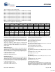
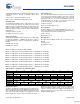
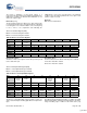
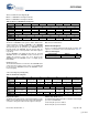
Table Of Contents
- EZ-Host Features
- Typical Applications
- Introduction
- Functional Overview
- Interface Descriptions
- USB Interface
- OTG Interface
- External Memory Interface
- General Purpose IO Interface (GPIO)
- UART Interface
- I2C EEPROM Interface
- Serial Peripheral Interface
- High-Speed Serial Interface
- Programmable Pulse/PWM Interface
- Host Port Interface
- IDE Interface
- Charge Pump Interface
- Booster Interface
- Crystal Interface
- Boot Configuration Interface
- Operational Modes
- Power Savings and Reset Description
- Memory Map
- Registers
- Processor Control Registers
- CPU Flags Register [0xC000] [R]
- Bank Register [0xC002] [R/W]
- Hardware Revision Register [0xC004] [R]
- CPU Speed Register [0xC008] [R/W]
- Power Control Register [0xC00A] [R/W]
- Interrupt Enable Register [0xC00E] [R/W]
- Breakpoint Register [0xC014] [R/W]
- USB Diagnostic Register [0xC03C] [R/W]
- Memory Diagnostic Register [0xC03E] [W]
- External Memory Registers
- Timer Registers
- General USB Registers
- USB Host Only Registers
- Host n Control Register [R/W]
- Host n Address Register [R/W]
- Host n Count Register [R/W]
- Host n Endpoint Status Register [R]
- Host n PID Register [W]
- Host n Count Result Register [R]
- Host n Device Address Register [W]
- Host n Interrupt Enable Register [R/W]
- Host n Status Register [R/W]
- Host n SOF/EOP Count Register [R/W]
- Host n SOF/EOP Counter Register [R]
- Host n Frame Register [R]
- USB Device Only Registers
- Device n Endpoint n Control Register [R/W]
- Device n Endpoint n Address Register [R/W]
- Device n Endpoint n Count Register [R/W]
- Device n Endpoint n Status Register [R/W]
- Device n Endpoint n Count Result Register [R/W]
- Device n Port Select Register [R/W]
- Device n Interrupt Enable Register [R/W]
- Device n Address Register [W]
- Device n Status Register [R/W]
- Device n Frame Number Register [R]
- Device n SOF/EOP Count Register [W]
- OTG Control Registers
- GPIO Registers
- IDE Registers
- HSS Registers
- HSS Control Register [0xC070] [R/W]
- HSS Baud Rate Register [0xC072] [R/W]
- HSS Transmit Gap Register [0xC074] [R/W]
- HSS Data Register [0xC076] [R/W]
- HSS Receive Address Register [0xC078] [R/W]
- HSS Receive Counter Register [0xC07A] [R/W]
- HSS Transmit Address Register [0xC07C] [R/W]
- HSS Transmit Counter Register [0xC07E] [R/W]
- HPI Registers
- SPI Registers
- SPI Configuration Register [0xC0C8] [R/W]
- SPI Control Register [0xC0CA] [R/W]
- SPI Interrupt Enable Register [0xC0CC] [R/W]
- SPI Status Register [0xC0CE] [R]
- SPI Interrupt Clear Register [0xC0D0] [W]
- SPI CRC Control Register [0xC0D2] [R/W]
- SPI CRC Value Register [0xC0D4] [R/W]
- SPI Data Register [0xC0D6] [R/W]
- SPI Transmit Address Register [0xC0D8] [R/W]
- SPI Transmit Count Register [0xC0DA] [R/W]
- SPI Receive Address Register [0xC0DC [R/W]
- SPI Receive Count Register [0xC0DE] [R/W]
- UART Registers
- PWM Registers
- Processor Control Registers
- Pin Diagram
- Pin Descriptions
- Absolute Maximum Ratings
- Operating Conditions
- Crystal Requirements (XTALIN, XTALOUT)
- DC Characteristics
- AC Timing Characteristics
- Register Summary
- Ordering Information
- Package Diagrams
- Document History Page
- Sales, Solutions, and Legal Information
CY7C67300
Document #: 38-08015 Rev. *J Page 48 of 99
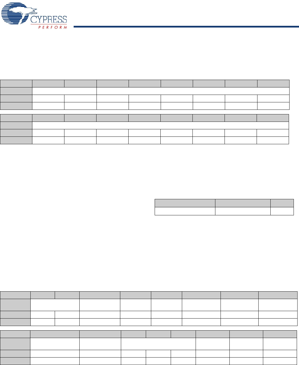
Device n SOF/EOP Count Register [W]
■ Device 1 SOF/EOP Count Register 0xC094
■ Device 2 SOF/EOP Count Register 0xC0B4
Register Description
The Device n SOF/EOP Count register is written with the time
expected between receiving a SOF/EOP. If the SOF/EOP
counter expires before an SOF/EOP is received, an SOF/EOP
Timeout Interrupt can be generated. The SOF/EOP Timeout
Interrupt Enable and SOF/EOP Timeout Interrupt Flag are
located in the Device n Interrupt Enable and Status registers
respectively.
Set the SOF/EOP count slightly greater than the expected
SOF/EOP interval. The SOF/EOP counter decrements at a
12 MHz rate. Therefore, in the case of an expected 1 ms
SOF/EOP interval, the SOF/EOP count is set slightly greater
than 0x2EE0.
Count (Bits [13:0])
The Count field contains the current value of the SOF/EOP down
counter. At power up and reset, this value is set to 0x2EE0 and
for expected 1 ms SOF/EOP intervals, this SOF/EOP count is
increased slightly.
Reserved
Write all reserved bits with ’0’.
OTG Control Registers
There is one register dedicated for On-The-Go operation. This
register is covered in this section and summarized in Table 74.
OTG Control Register [0xC098] [R/W]
Register Description
The OTG Control register allows control and monitoring over the
OTG port on Port1A. Note that the D± pull up and pull down bits
override the setting in the USB 0 Control register for this port.
VBUS Pull-up Enable (Bit 13)
The VBUS Pull-up Enable bit enables or disables a 500 ohm pull
up resistor onto OTG VBus.
1: 500 ohm pull up resistor enabled
0: 500 ohm pull up resistor disabled
Table 73. Device n SOF/EOP Count Register
Bit # 15 14 13 12 11 10 9 8
Field Reserved Count...
Read/Write - - R R R R R R
Default 0 0 1 0 1 1 1 0
Bit # 7 6 5 4 3 2 1 0
Field ...Count
Read/Write R R R R R R R R
Default 1 1 1 0 0 0 0 0
Table 74. OTG Register
Register Name Address R/W
OTG Control Register C098H R/W
Table 75. OTG Control Register
Bit # 15 14 13 12 11 10 9 8
Field
Reserved VBUS
Pull-up Enable
Receive
Disable
Charge Pump
Enable
VBUS
Discharge Enable
D+
Pull-up Enable
D–
Pull-up Enable
Read/Write - - R/W R/W R/W R/W R/W R/W
Default 0 0 0 0 0 0 0 0
Bit # 7 6 5 4 3 2 1 0
Field
D+
Pull-down Enable
D–
Pull-down Enable
Reserved OTG Data
Status
ID
Status
VBUS Valid
Flag
Read/Write R/W R/W - - - R R R
Default 0 0 0 0 0 X X X
[+] Feedback