
Programmable Embedded USB Host and Peripheral Controller with Automotive AEC Grade Support Specification Sheet
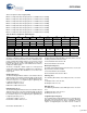
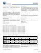
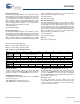
Table Of Contents
- EZ-Host Features
- Typical Applications
- Introduction
- Functional Overview
- Interface Descriptions
- USB Interface
- OTG Interface
- External Memory Interface
- General Purpose IO Interface (GPIO)
- UART Interface
- I2C EEPROM Interface
- Serial Peripheral Interface
- High-Speed Serial Interface
- Programmable Pulse/PWM Interface
- Host Port Interface
- IDE Interface
- Charge Pump Interface
- Booster Interface
- Crystal Interface
- Boot Configuration Interface
- Operational Modes
- Power Savings and Reset Description
- Memory Map
- Registers
- Processor Control Registers
- CPU Flags Register [0xC000] [R]
- Bank Register [0xC002] [R/W]
- Hardware Revision Register [0xC004] [R]
- CPU Speed Register [0xC008] [R/W]
- Power Control Register [0xC00A] [R/W]
- Interrupt Enable Register [0xC00E] [R/W]
- Breakpoint Register [0xC014] [R/W]
- USB Diagnostic Register [0xC03C] [R/W]
- Memory Diagnostic Register [0xC03E] [W]
- External Memory Registers
- Timer Registers
- General USB Registers
- USB Host Only Registers
- Host n Control Register [R/W]
- Host n Address Register [R/W]
- Host n Count Register [R/W]
- Host n Endpoint Status Register [R]
- Host n PID Register [W]
- Host n Count Result Register [R]
- Host n Device Address Register [W]
- Host n Interrupt Enable Register [R/W]
- Host n Status Register [R/W]
- Host n SOF/EOP Count Register [R/W]
- Host n SOF/EOP Counter Register [R]
- Host n Frame Register [R]
- USB Device Only Registers
- Device n Endpoint n Control Register [R/W]
- Device n Endpoint n Address Register [R/W]
- Device n Endpoint n Count Register [R/W]
- Device n Endpoint n Status Register [R/W]
- Device n Endpoint n Count Result Register [R/W]
- Device n Port Select Register [R/W]
- Device n Interrupt Enable Register [R/W]
- Device n Address Register [W]
- Device n Status Register [R/W]
- Device n Frame Number Register [R]
- Device n SOF/EOP Count Register [W]
- OTG Control Registers
- GPIO Registers
- IDE Registers
- HSS Registers
- HSS Control Register [0xC070] [R/W]
- HSS Baud Rate Register [0xC072] [R/W]
- HSS Transmit Gap Register [0xC074] [R/W]
- HSS Data Register [0xC076] [R/W]
- HSS Receive Address Register [0xC078] [R/W]
- HSS Receive Counter Register [0xC07A] [R/W]
- HSS Transmit Address Register [0xC07C] [R/W]
- HSS Transmit Counter Register [0xC07E] [R/W]
- HPI Registers
- SPI Registers
- SPI Configuration Register [0xC0C8] [R/W]
- SPI Control Register [0xC0CA] [R/W]
- SPI Interrupt Enable Register [0xC0CC] [R/W]
- SPI Status Register [0xC0CE] [R]
- SPI Interrupt Clear Register [0xC0D0] [W]
- SPI CRC Control Register [0xC0D2] [R/W]
- SPI CRC Value Register [0xC0D4] [R/W]
- SPI Data Register [0xC0D6] [R/W]
- SPI Transmit Address Register [0xC0D8] [R/W]
- SPI Transmit Count Register [0xC0DA] [R/W]
- SPI Receive Address Register [0xC0DC [R/W]
- SPI Receive Count Register [0xC0DE] [R/W]
- UART Registers
- PWM Registers
- Processor Control Registers
- Pin Diagram
- Pin Descriptions
- Absolute Maximum Ratings
- Operating Conditions
- Crystal Requirements (XTALIN, XTALOUT)
- DC Characteristics
- AC Timing Characteristics
- Register Summary
- Ordering Information
- Package Diagrams
- Document History Page
- Sales, Solutions, and Legal Information
CY7C67300
Document #: 38-08015 Rev. *J Page 45 of 99
Error, or OUT Exception Error. In addition, the NAK Interrupt
Enable bit in the Device n Endpoint Control register can also be
set so that NAK responses trigger this interrupt.
1: Enable EP1 Transaction Done interrupt
0: Disable EP1 Transaction Done interrupt
EP0 Interrupt Enable (Bit 0)
The EP0 Interrupt Enable bit enables or disables endpoint zero
(EP0) Transaction Done interrupt. An EPx Transaction Done
interrupt triggers when any of the following responses or events
occur in a transaction for the device’s supplied Endpoint:
send/receive ACK, send STALL, Timeout occurs, IN Exception
Error, or OUT Exception Error. In addition, the NAK Interrupt
Enable bit in the Device n Endpoint Control register can also be
set so that NAK responses trigger this interrupt.
1: Enable EP0 Transaction Done interrupt
0: Disable EP0 Transaction Done interrupt
Reserved
Write all reserved bits with ’0’.
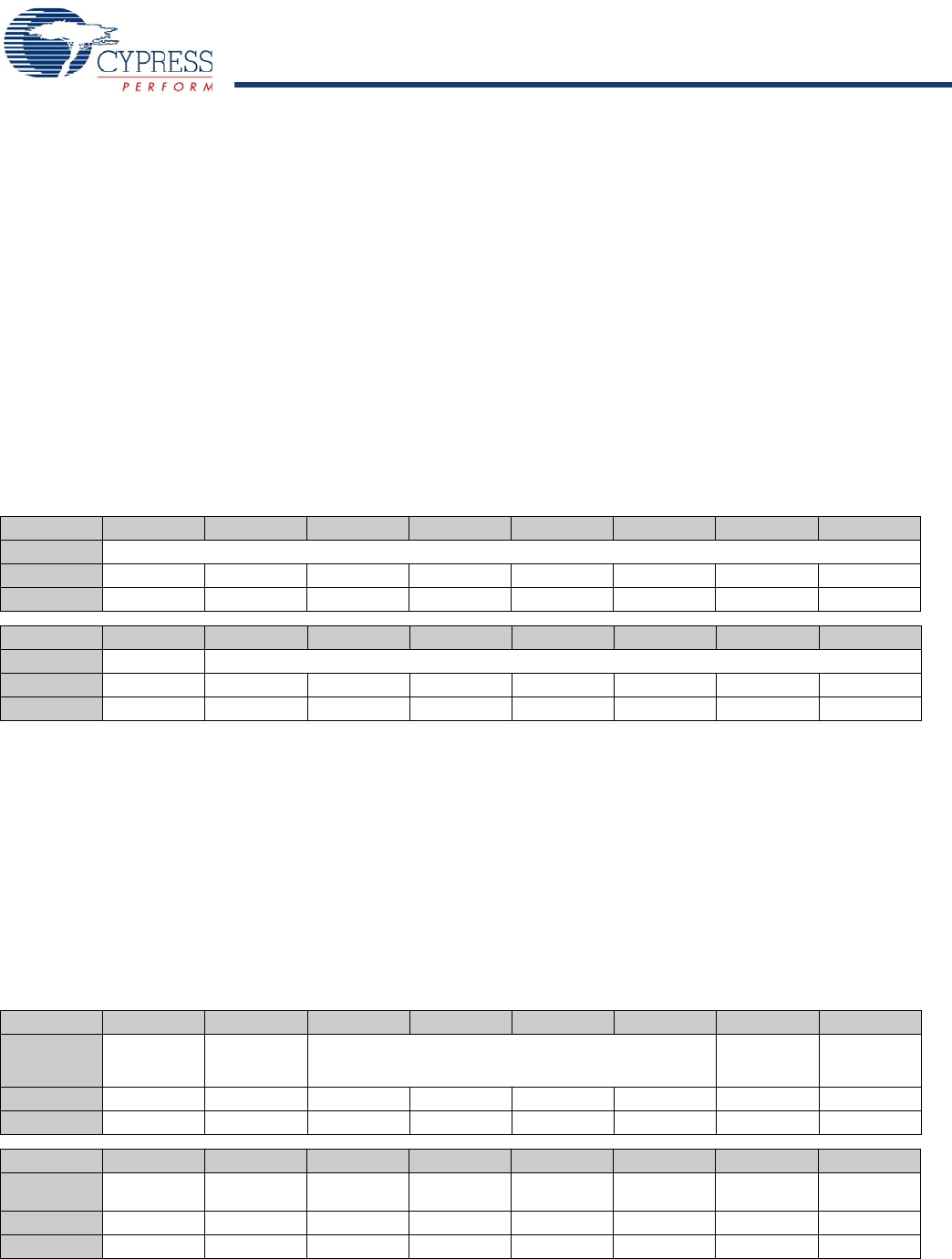
Device n Address Register [W]
■ Device 1 Address Register 0xC08E
■ Device 2 Address Register 0xC0AE
Register Description
The Device n Address register holds the device address
assigned by the host. This register initializes to the default
address 0 at reset but must be updated by firmware when the
host assigns a new address. Only USB data sent to the address
contained in this register gets a respond—all others are ignored.
Address (Bits [6:0])
The Address field contains the USB address of the device
assigned by the host.
Reserved
Write all reserved bits with ’0’.
Device n Status Register [R/W]
■ Device 1 Status Register 0xC090
■ Device 2 Status Register 0xC0B0
Table 70. Device n Address Register
Bit # 15 14 13 12 11 10 9 8
Field Reserved...
Read/Write - - - - - - - -
Default 0 0 0 0 0 0 0 0
Bit # 7 6 5 4 3 2 1 0
Field ...Reserved Address
Read/Write - W W W W W W W
Default 0 0 0 0 0 0 0 0
Table 71. Device n Status Register
Bit # 15 14 13 12 11 10 9 8
Field
VBUS Inter-
rupt
Flag
ID Interrupt
Flag
Reserved SOF/EOP
Interrupt Flag
Reset Interrupt
Flag
Read/Write R/W R/W - - - - R/W R/W
Default X X X X X X X X
Bit # 7 6 5 4 3 2 1 0
Field
EP7 Interrupt
Flag
EP6 Interrupt
Flag
EP5 Interrupt
Flag
EP4 Interrupt
Flag
EP3 Interrupt
Flag
EP2 Interrupt
Flag
EP1 Interrupt
Flag
EP0 Interrupt
Flag
Read/Write R/W R/W R/W R/W R/W R/W R/W R/W
Default X X X X X X X X
[+] Feedback