
Programmable Embedded USB Host and Peripheral Controller with Automotive AEC Grade Support Specification Sheet
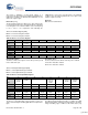
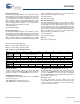
Table Of Contents
- EZ-Host Features
- Typical Applications
- Introduction
- Functional Overview
- Interface Descriptions
- USB Interface
- OTG Interface
- External Memory Interface
- General Purpose IO Interface (GPIO)
- UART Interface
- I2C EEPROM Interface
- Serial Peripheral Interface
- High-Speed Serial Interface
- Programmable Pulse/PWM Interface
- Host Port Interface
- IDE Interface
- Charge Pump Interface
- Booster Interface
- Crystal Interface
- Boot Configuration Interface
- Operational Modes
- Power Savings and Reset Description
- Memory Map
- Registers
- Processor Control Registers
- CPU Flags Register [0xC000] [R]
- Bank Register [0xC002] [R/W]
- Hardware Revision Register [0xC004] [R]
- CPU Speed Register [0xC008] [R/W]
- Power Control Register [0xC00A] [R/W]
- Interrupt Enable Register [0xC00E] [R/W]
- Breakpoint Register [0xC014] [R/W]
- USB Diagnostic Register [0xC03C] [R/W]
- Memory Diagnostic Register [0xC03E] [W]
- External Memory Registers
- Timer Registers
- General USB Registers
- USB Host Only Registers
- Host n Control Register [R/W]
- Host n Address Register [R/W]
- Host n Count Register [R/W]
- Host n Endpoint Status Register [R]
- Host n PID Register [W]
- Host n Count Result Register [R]
- Host n Device Address Register [W]
- Host n Interrupt Enable Register [R/W]
- Host n Status Register [R/W]
- Host n SOF/EOP Count Register [R/W]
- Host n SOF/EOP Counter Register [R]
- Host n Frame Register [R]
- USB Device Only Registers
- Device n Endpoint n Control Register [R/W]
- Device n Endpoint n Address Register [R/W]
- Device n Endpoint n Count Register [R/W]
- Device n Endpoint n Status Register [R/W]
- Device n Endpoint n Count Result Register [R/W]
- Device n Port Select Register [R/W]
- Device n Interrupt Enable Register [R/W]
- Device n Address Register [W]
- Device n Status Register [R/W]
- Device n Frame Number Register [R]
- Device n SOF/EOP Count Register [W]
- OTG Control Registers
- GPIO Registers
- IDE Registers
- HSS Registers
- HSS Control Register [0xC070] [R/W]
- HSS Baud Rate Register [0xC072] [R/W]
- HSS Transmit Gap Register [0xC074] [R/W]
- HSS Data Register [0xC076] [R/W]
- HSS Receive Address Register [0xC078] [R/W]
- HSS Receive Counter Register [0xC07A] [R/W]
- HSS Transmit Address Register [0xC07C] [R/W]
- HSS Transmit Counter Register [0xC07E] [R/W]
- HPI Registers
- SPI Registers
- SPI Configuration Register [0xC0C8] [R/W]
- SPI Control Register [0xC0CA] [R/W]
- SPI Interrupt Enable Register [0xC0CC] [R/W]
- SPI Status Register [0xC0CE] [R]
- SPI Interrupt Clear Register [0xC0D0] [W]
- SPI CRC Control Register [0xC0D2] [R/W]
- SPI CRC Value Register [0xC0D4] [R/W]
- SPI Data Register [0xC0D6] [R/W]
- SPI Transmit Address Register [0xC0D8] [R/W]
- SPI Transmit Count Register [0xC0DA] [R/W]
- SPI Receive Address Register [0xC0DC [R/W]
- SPI Receive Count Register [0xC0DE] [R/W]
- UART Registers
- PWM Registers
- Processor Control Registers
- Pin Diagram
- Pin Descriptions
- Absolute Maximum Ratings
- Operating Conditions
- Crystal Requirements (XTALIN, XTALOUT)
- DC Characteristics
- AC Timing Characteristics
- Register Summary
- Ordering Information
- Package Diagrams
- Document History Page
- Sales, Solutions, and Legal Information
CY7C67300
Document #: 38-08015 Rev. *J Page 42 of 99
underflow and the Overflow and Underflow flags (bits 11 and 10
respectively) must be checked to determine which event
occurred.
1: An overflow or underflow condition occurred
0: An overflow or underflow condition did not occur
Setup Flag (Bit 4)
The Setup Flag bit indicates that a setup packet was received.
In device mode setup packets are stored at memory location
0x0300 for Device 1 and 0x0308 for Device 2. Setup packets are
always accepted regardless of the Direction Select and Arm
Enable bit settings as long as the Device n EP n Control register
Enable bit is set.
1: Setup packet was received
0: Setup packet was not received
Sequence Flag (Bit 3)
The Sequence Flag bit indicates whether the last data toggle
received was a DATA1 or a DATA0. This bit has no effect on
receiving data packets; sequence checking must be handled in
firmware.
1: DATA1 was received
0: DATA0 was received
Timeout Flag (Bit 2)
The Timeout Flag bit indicates whether a timeout condition
occurred on the last transaction. On the device side, a timeout
can occur if the device sends a data packet in response to an IN
request but then does not receive a handshake packet in a
predetermined time. It can also occur if the device does not
receive the data stage of an OUT transfer in time.
1: Timeout occurred
0: Timeout condition did not occur
Error Flag (Bit 2)
The Error Flag bit is set if a CRC5 and CRC16 error occurs, or if
an incorrect packet type is received. Overflow and underflow are
not considered errors and do not affect this bit.
1: Error occurred
0: Error did not occur
ACK Flag (Bit 0)
The ACK Flag bit indicates whether the last transaction was
ACKed.
1: ACK occurred
0: ACK did not occur
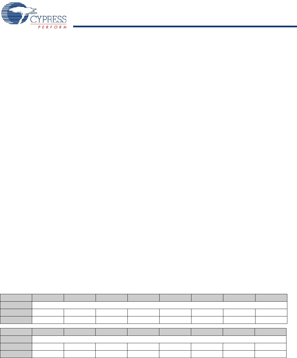
Device n Endpoint n Count Result Register [R/W]
■ Device n Endpoint 0 Count Result Register [Device 1: 0x0208 Device 2: 0x0288]
■ Device n Endpoint 1 Count Result Register [Device 1: 0x0218 Device 2: 0x0298]
■ Device n Endpoint 2 Count Result Register [Device 1: 0x0228 Device 2: 0x02A8]
■ Device n Endpoint 3 Count Result Register [Device 1: 0x0238 Device 2: 0x02B8]
■ Device n Endpoint 4 Count Result Register [Device 1: 0x0248 Device 2: 0x02C8]
■ Device n Endpoint 5 Count Result Register [Device 1: 0x0258 Device 2: 0x02D8]
■ Device n Endpoint 6 Count Result Register [Device 1: 0x0268 Device 2: 0x02E8]
■ Device n Endpoint 7 Count Result Register [Device 1: 0x0278 Device 2: 0x02F8]
Register Description
The Device n Endpoint n Count Result register contains the size
difference in bytes between the Endpoint Count specified in the
Device n Endpoint n Count register and the last packet received.
If an overflow or underflow condition occurs, that is, the received
packet length differs from the value specified in the Device n
Endpoint n Count register, the Length Exception Flag bit in the
Device n Endpoint n Status register is set. The value in this
register is only valued when the Length Exception Flag bit is set
and the Error Flag bit is not set; both bits are in the Device n
Endpoint n Status register.
Table 67. Device n Endpoint n Count Result Register
Bit # 15 14 13 12 11 10 9 8
Field Result...
Read/Write R/W R/W R/W R/W R/W R/W R/W R/W
Default X X X X X X X X
Bit # 7 6 5 4 3 2 1 0
Field ...Result
Read/Write R/W R/W R/W R/W R/W R/W R/W R/W
Default X X X X X X X X
[+] Feedback