
Programmable Embedded USB Host and Peripheral Controller with Automotive AEC Grade Support Specification Sheet
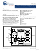
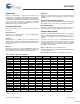
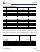
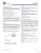
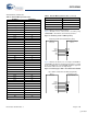
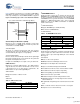
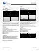
Table Of Contents
- EZ-Host Features
- Typical Applications
- Introduction
- Functional Overview
- Interface Descriptions
- USB Interface
- OTG Interface
- External Memory Interface
- General Purpose IO Interface (GPIO)
- UART Interface
- I2C EEPROM Interface
- Serial Peripheral Interface
- High-Speed Serial Interface
- Programmable Pulse/PWM Interface
- Host Port Interface
- IDE Interface
- Charge Pump Interface
- Booster Interface
- Crystal Interface
- Boot Configuration Interface
- Operational Modes
- Power Savings and Reset Description
- Memory Map
- Registers
- Processor Control Registers
- CPU Flags Register [0xC000] [R]
- Bank Register [0xC002] [R/W]
- Hardware Revision Register [0xC004] [R]
- CPU Speed Register [0xC008] [R/W]
- Power Control Register [0xC00A] [R/W]
- Interrupt Enable Register [0xC00E] [R/W]
- Breakpoint Register [0xC014] [R/W]
- USB Diagnostic Register [0xC03C] [R/W]
- Memory Diagnostic Register [0xC03E] [W]
- External Memory Registers
- Timer Registers
- General USB Registers
- USB Host Only Registers
- Host n Control Register [R/W]
- Host n Address Register [R/W]
- Host n Count Register [R/W]
- Host n Endpoint Status Register [R]
- Host n PID Register [W]
- Host n Count Result Register [R]
- Host n Device Address Register [W]
- Host n Interrupt Enable Register [R/W]
- Host n Status Register [R/W]
- Host n SOF/EOP Count Register [R/W]
- Host n SOF/EOP Counter Register [R]
- Host n Frame Register [R]
- USB Device Only Registers
- Device n Endpoint n Control Register [R/W]
- Device n Endpoint n Address Register [R/W]
- Device n Endpoint n Count Register [R/W]
- Device n Endpoint n Status Register [R/W]
- Device n Endpoint n Count Result Register [R/W]
- Device n Port Select Register [R/W]
- Device n Interrupt Enable Register [R/W]
- Device n Address Register [W]
- Device n Status Register [R/W]
- Device n Frame Number Register [R]
- Device n SOF/EOP Count Register [W]
- OTG Control Registers
- GPIO Registers
- IDE Registers
- HSS Registers
- HSS Control Register [0xC070] [R/W]
- HSS Baud Rate Register [0xC072] [R/W]
- HSS Transmit Gap Register [0xC074] [R/W]
- HSS Data Register [0xC076] [R/W]
- HSS Receive Address Register [0xC078] [R/W]
- HSS Receive Counter Register [0xC07A] [R/W]
- HSS Transmit Address Register [0xC07C] [R/W]
- HSS Transmit Counter Register [0xC07E] [R/W]
- HPI Registers
- SPI Registers
- SPI Configuration Register [0xC0C8] [R/W]
- SPI Control Register [0xC0CA] [R/W]
- SPI Interrupt Enable Register [0xC0CC] [R/W]
- SPI Status Register [0xC0CE] [R]
- SPI Interrupt Clear Register [0xC0D0] [W]
- SPI CRC Control Register [0xC0D2] [R/W]
- SPI CRC Value Register [0xC0D4] [R/W]
- SPI Data Register [0xC0D6] [R/W]
- SPI Transmit Address Register [0xC0D8] [R/W]
- SPI Transmit Count Register [0xC0DA] [R/W]
- SPI Receive Address Register [0xC0DC [R/W]
- SPI Receive Count Register [0xC0DE] [R/W]
- UART Registers
- PWM Registers
- Processor Control Registers
- Pin Diagram
- Pin Descriptions
- Absolute Maximum Ratings
- Operating Conditions
- Crystal Requirements (XTALIN, XTALOUT)
- DC Characteristics
- AC Timing Characteristics
- Register Summary
- Ordering Information
- Package Diagrams
- Document History Page
- Sales, Solutions, and Legal Information
CY7C67300
Document #: 38-08015 Rev. *J Page 4 of 99
USB Features
■ USB 2.0-compliant for full and low speed
■ Up to four downstream USB host ports
■ Up to two upstream USB peripheral ports
■ Configurable endpoint buffers (pointer and length), must reside
in internal RAM
■ Up to eight available peripheral endpoints (one control
endpoint)
■ Supports control, interrupt, bulk, and isochronous transfers
■ Internal DMA channels for each endpoint
■ Internal pull up and pull down resistors
■ Internal series termination resistors on USB data lines
USB Pins
OTG Interface
EZ-Host has one USB port that is compatible with the USB
On-The-Go supplement to the USB 2.0 specification. The USB
OTG port has a various hardware features to support Session
Request Protocol (SRP) and Host Negotiation Protocol (HNP).
OTG is only supported on USB PORT 1A.
OTG Features
■ Internal charge pump to supply and control VBUS
■ VBUS valid status (above 4.4V)
■ VBUS status for 2.4V< VBUS <0.8V
■ ID pin status
■ Switchable 2K ohm internal discharge resistor on VBUS
■ Switchable 500 ohm internal pull up resistor on VBUS
■ Individually switchable internal pull up and pull down resistors
on the USB data lines
OTG Pins
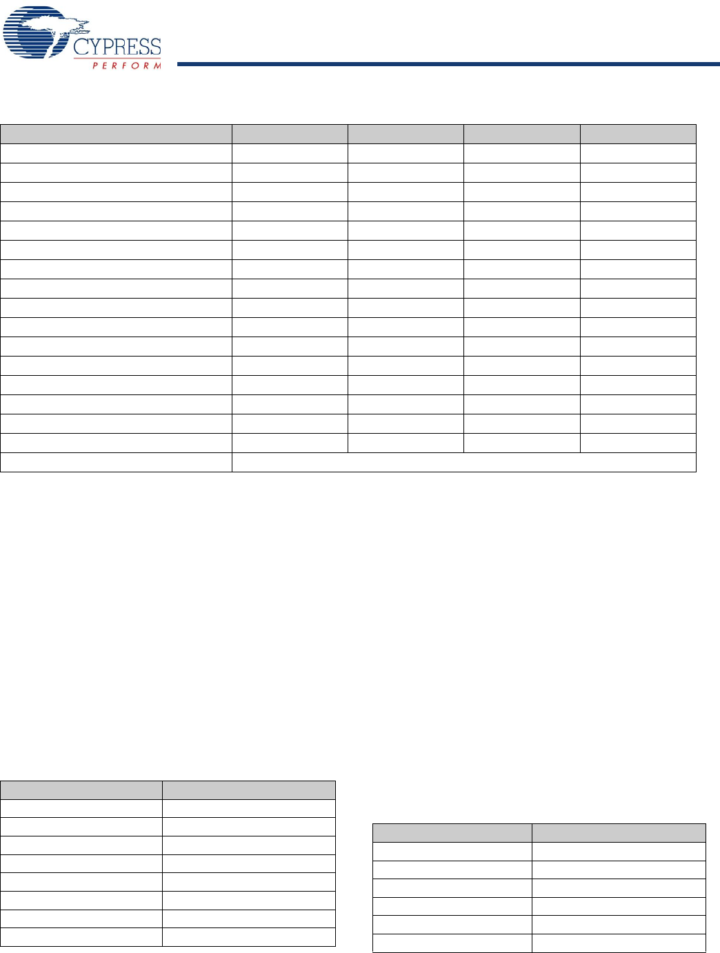
2 Hosts + 1 Peripheral Host Host Peripheral –
2 Hosts + 1 Peripheral Host Host – Peripheral
2 Hosts + 1 Peripheral Peripheral – Host Host
2 Hosts + 1 Peripheral – Peripheral Host Host
1 Host + 1 Peripheral Host – Peripheral –
1 Host + 1 Peripheral Host – – Peripheral
1 Host + 1 Peripheral – Host – Peripheral
1 Host + 1 Peripheral – Host Peripheral –
1 Host + 1 Peripheral Peripheral – Host –
1 Host + 1 Peripheral Peripheral – – Host
1 Host + 1 Peripheral – Peripheral – Host
1 Host + 1 Peripheral – Peripheral Host –
2 Peripherals Peripheral – Peripheral –
2 Peripherals Peripheral – – Peripheral
2 Peripherals – Peripheral – Peripheral
2 Peripherals – Peripheral Peripheral –
1 Peripheral Any Port
Table 3. USB Port Configuration Options (continued)
Port Configurations Port 1A Port 1B Port 2A Port 2B
Table 4. USB Interface Pins
Pin Name Pin Number
DM1A 22
DP1A 23
DM1B 18
DP1B 19
DM2A 9
DP2A 10
DM2B 4
DP2B 5
Table 5. OTG Interface Pins
Pin Name Pin Number
DM1A 22
DP1A 23
OTGVBUS 11
OTGID 41
CSwitchA 13
CSwitchB 12
[+] Feedback