
Programmable Embedded USB Host and Peripheral Controller with Automotive AEC Grade Support Specification Sheet
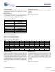
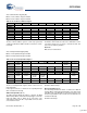
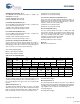
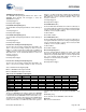
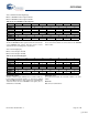
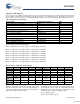
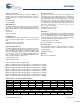
Table Of Contents
- EZ-Host Features
- Typical Applications
- Introduction
- Functional Overview
- Interface Descriptions
- USB Interface
- OTG Interface
- External Memory Interface
- General Purpose IO Interface (GPIO)
- UART Interface
- I2C EEPROM Interface
- Serial Peripheral Interface
- High-Speed Serial Interface
- Programmable Pulse/PWM Interface
- Host Port Interface
- IDE Interface
- Charge Pump Interface
- Booster Interface
- Crystal Interface
- Boot Configuration Interface
- Operational Modes
- Power Savings and Reset Description
- Memory Map
- Registers
- Processor Control Registers
- CPU Flags Register [0xC000] [R]
- Bank Register [0xC002] [R/W]
- Hardware Revision Register [0xC004] [R]
- CPU Speed Register [0xC008] [R/W]
- Power Control Register [0xC00A] [R/W]
- Interrupt Enable Register [0xC00E] [R/W]
- Breakpoint Register [0xC014] [R/W]
- USB Diagnostic Register [0xC03C] [R/W]
- Memory Diagnostic Register [0xC03E] [W]
- External Memory Registers
- Timer Registers
- General USB Registers
- USB Host Only Registers
- Host n Control Register [R/W]
- Host n Address Register [R/W]
- Host n Count Register [R/W]
- Host n Endpoint Status Register [R]
- Host n PID Register [W]
- Host n Count Result Register [R]
- Host n Device Address Register [W]
- Host n Interrupt Enable Register [R/W]
- Host n Status Register [R/W]
- Host n SOF/EOP Count Register [R/W]
- Host n SOF/EOP Counter Register [R]
- Host n Frame Register [R]
- USB Device Only Registers
- Device n Endpoint n Control Register [R/W]
- Device n Endpoint n Address Register [R/W]
- Device n Endpoint n Count Register [R/W]
- Device n Endpoint n Status Register [R/W]
- Device n Endpoint n Count Result Register [R/W]
- Device n Port Select Register [R/W]
- Device n Interrupt Enable Register [R/W]
- Device n Address Register [W]
- Device n Status Register [R/W]
- Device n Frame Number Register [R]
- Device n SOF/EOP Count Register [W]
- OTG Control Registers
- GPIO Registers
- IDE Registers
- HSS Registers
- HSS Control Register [0xC070] [R/W]
- HSS Baud Rate Register [0xC072] [R/W]
- HSS Transmit Gap Register [0xC074] [R/W]
- HSS Data Register [0xC076] [R/W]
- HSS Receive Address Register [0xC078] [R/W]
- HSS Receive Counter Register [0xC07A] [R/W]
- HSS Transmit Address Register [0xC07C] [R/W]
- HSS Transmit Counter Register [0xC07E] [R/W]
- HPI Registers
- SPI Registers
- SPI Configuration Register [0xC0C8] [R/W]
- SPI Control Register [0xC0CA] [R/W]
- SPI Interrupt Enable Register [0xC0CC] [R/W]
- SPI Status Register [0xC0CE] [R]
- SPI Interrupt Clear Register [0xC0D0] [W]
- SPI CRC Control Register [0xC0D2] [R/W]
- SPI CRC Value Register [0xC0D4] [R/W]
- SPI Data Register [0xC0D6] [R/W]
- SPI Transmit Address Register [0xC0D8] [R/W]
- SPI Transmit Count Register [0xC0DA] [R/W]
- SPI Receive Address Register [0xC0DC [R/W]
- SPI Receive Count Register [0xC0DE] [R/W]
- UART Registers
- PWM Registers
- Processor Control Registers
- Pin Diagram
- Pin Descriptions
- Absolute Maximum Ratings
- Operating Conditions
- Crystal Requirements (XTALIN, XTALOUT)
- DC Characteristics
- AC Timing Characteristics
- Register Summary
- Ordering Information
- Package Diagrams
- Document History Page
- Sales, Solutions, and Legal Information

CY7C67300
Document #: 38-08015 Rev. *J Page 39 of 99
Sequence Select (Bit 6)
The Sequence Select bit determines whether a DATA0 or a
DATA1 is sent for the next data toggle. This bit has no effect on
receiving data packets; sequence checking must be handled in
firmware.
1: Send a DATA1
0: Send a DATA0
Stall Enable (Bit 5)
The Stall Enable bit sends a Stall in response to the next request
(unless it is a setup request, which are always ACKed). This is a
sticky bit and continues to respond with Stalls until cleared by
firmware.
1: Send Stall
0: Do not send Stall
ISO Enable (Bit 4)
The ISO Enable bit enables and disables an isochronous trans-
action. This bit is only valid for EPs 1–7 and has no function for
EP0.
1: Enable isochronous transaction
0: Disable isochronous transaction
NAK Interrupt Enable (Bit 3)
The NAK Interrupt Enable bit enables and disables the gener-
ation of an Endpoint n interrupt when the device responds to the
host with a NAK. The Endpoint n Interrupt Enable bit in the
Device n Interrupt Enable register must also be set. When a NAK
is sent to the host, the corresponding EP Interrupt Flag in the
Device n Status register is set. In addition, the NAK Flag in the
Device n Endpoint n Status register is set.
1: Enable NAK interrupt
0: Disable NAK interrupt
Direction Select (Bit 2)
The Direction Select bit needs to be set according to the
expected direction of the next data stage in the next transaction.
If the data stage direction is different from what is set in this bit,
it gets NAKed and either the IN Exception Flag or the OUT
Exception Flag is set in the Device n Endpoint n Status register.
If a setup packet is received and the Direction Select bit is set
incorrectly, the setup is ACKed and the Setup Status Flag is set
(refer to the setup bit of the Device n Endpoint n Status Register
[R/W] on page 41 for details).
1: OUT transfer (host to device)
0: IN transfer (device to host)
Enable (Bit 1)
Set the Enable bit to allow transfers to the endpoint. If Enable is
set to ‘0’ then all USB traffic to this endpoint is ignored. If Enable
is set ‘1’ and Arm Enable (bit 0) is set ‘0’ then NAKs are automat-
ically returned from this endpoint (except setup packets which
are always ACKed as long as the Enable bit is set).
1: Enable transfers to an endpoint
0: Do not allow transfers to an endpoint
Arm Enable (Bit 0)
The Arm Enable bit arms the endpoint to transfer or receive a
packet. This bit is cleared to ‘0’ when a transaction is complete.
1: Arm endpoint
0: Endpoint disarmed
Reserved
Write all reserved bits with ’0’.
Device n Endpoint n Address Register [R/W]
■ Device n Endpoint 0 Address Register [Device 1: 0x0202 Device 2: 0x0282]
■ Device n Endpoint 1 Address Register [Device 1: 0x0212 Device 2: 0x0292]
■ Device n Endpoint 2 Address Register [Device 1: 0x0222 Device 2: 0x02A2]
■ Device n Endpoint 3 Address Register [Device 1: 0x0232 Device 2: 0x02B2]
■ Device n Endpoint 4 Address Register [Device 1: 0x0242 Device 2: 0x02C2]
■ Device n Endpoint 5 Address Register [Device 1: 0x0252 Device 2: 0x02D2]
■ Device n Endpoint 6 Address Register [Device 1: 0x0262 Device 2: 0x02E2]
■ Device n Endpoint 7 Address Register [Device 1: 0x0272 Device 2: 0x02F2]
Table 64. Device n Endpoint n Address Register
Bit # 15 14 13 12 11 10 9 8
Field Address...
Read/Write R/W R/W R/W R/W R/W R/W R/W R/W
Default X X X X X X X X
Bit # 7 6 5 4 3 2 1 0
Field ...Address
Read/Write R/W R/W R/W R/W R/W R/W R/W R/W
Default X X X X X X X X
[+] Feedback