
Programmable Embedded USB Host and Peripheral Controller with Automotive AEC Grade Support Specification Sheet
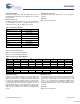
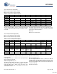
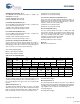
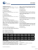
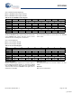
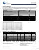
Table Of Contents
- EZ-Host Features
- Typical Applications
- Introduction
- Functional Overview
- Interface Descriptions
- USB Interface
- OTG Interface
- External Memory Interface
- General Purpose IO Interface (GPIO)
- UART Interface
- I2C EEPROM Interface
- Serial Peripheral Interface
- High-Speed Serial Interface
- Programmable Pulse/PWM Interface
- Host Port Interface
- IDE Interface
- Charge Pump Interface
- Booster Interface
- Crystal Interface
- Boot Configuration Interface
- Operational Modes
- Power Savings and Reset Description
- Memory Map
- Registers
- Processor Control Registers
- CPU Flags Register [0xC000] [R]
- Bank Register [0xC002] [R/W]
- Hardware Revision Register [0xC004] [R]
- CPU Speed Register [0xC008] [R/W]
- Power Control Register [0xC00A] [R/W]
- Interrupt Enable Register [0xC00E] [R/W]
- Breakpoint Register [0xC014] [R/W]
- USB Diagnostic Register [0xC03C] [R/W]
- Memory Diagnostic Register [0xC03E] [W]
- External Memory Registers
- Timer Registers
- General USB Registers
- USB Host Only Registers
- Host n Control Register [R/W]
- Host n Address Register [R/W]
- Host n Count Register [R/W]
- Host n Endpoint Status Register [R]
- Host n PID Register [W]
- Host n Count Result Register [R]
- Host n Device Address Register [W]
- Host n Interrupt Enable Register [R/W]
- Host n Status Register [R/W]
- Host n SOF/EOP Count Register [R/W]
- Host n SOF/EOP Counter Register [R]
- Host n Frame Register [R]
- USB Device Only Registers
- Device n Endpoint n Control Register [R/W]
- Device n Endpoint n Address Register [R/W]
- Device n Endpoint n Count Register [R/W]
- Device n Endpoint n Status Register [R/W]
- Device n Endpoint n Count Result Register [R/W]
- Device n Port Select Register [R/W]
- Device n Interrupt Enable Register [R/W]
- Device n Address Register [W]
- Device n Status Register [R/W]
- Device n Frame Number Register [R]
- Device n SOF/EOP Count Register [W]
- OTG Control Registers
- GPIO Registers
- IDE Registers
- HSS Registers
- HSS Control Register [0xC070] [R/W]
- HSS Baud Rate Register [0xC072] [R/W]
- HSS Transmit Gap Register [0xC074] [R/W]
- HSS Data Register [0xC076] [R/W]
- HSS Receive Address Register [0xC078] [R/W]
- HSS Receive Counter Register [0xC07A] [R/W]
- HSS Transmit Address Register [0xC07C] [R/W]
- HSS Transmit Counter Register [0xC07E] [R/W]
- HPI Registers
- SPI Registers
- SPI Configuration Register [0xC0C8] [R/W]
- SPI Control Register [0xC0CA] [R/W]
- SPI Interrupt Enable Register [0xC0CC] [R/W]
- SPI Status Register [0xC0CE] [R]
- SPI Interrupt Clear Register [0xC0D0] [W]
- SPI CRC Control Register [0xC0D2] [R/W]
- SPI CRC Value Register [0xC0D4] [R/W]
- SPI Data Register [0xC0D6] [R/W]
- SPI Transmit Address Register [0xC0D8] [R/W]
- SPI Transmit Count Register [0xC0DA] [R/W]
- SPI Receive Address Register [0xC0DC [R/W]
- SPI Receive Count Register [0xC0DE] [R/W]
- UART Registers
- PWM Registers
- Processor Control Registers
- Pin Diagram
- Pin Descriptions
- Absolute Maximum Ratings
- Operating Conditions
- Crystal Requirements (XTALIN, XTALOUT)
- DC Characteristics
- AC Timing Characteristics
- Register Summary
- Ordering Information
- Package Diagrams
- Document History Page
- Sales, Solutions, and Legal Information
CY7C67300
Document #: 38-08015 Rev. *J Page 38 of 99
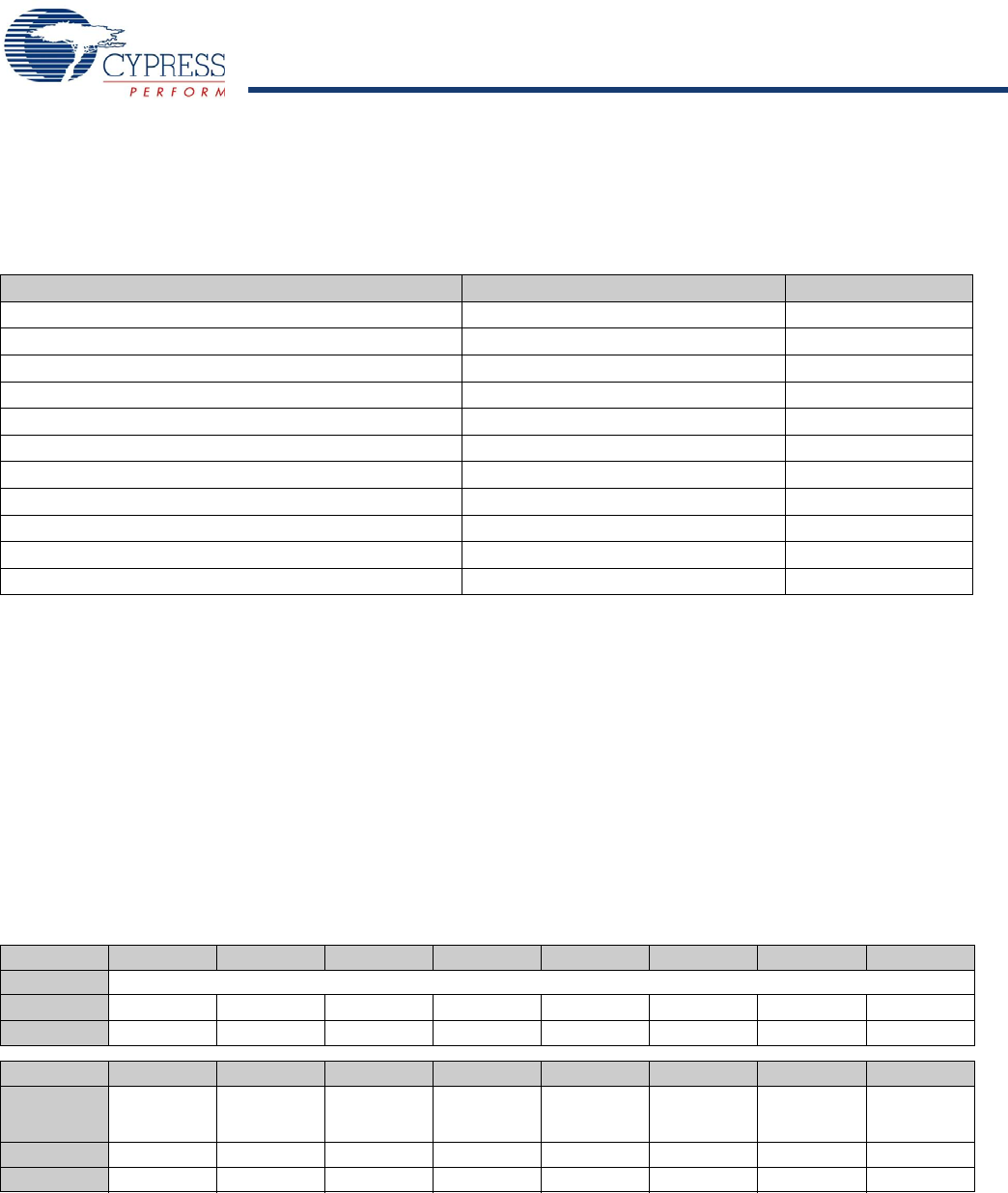
USB Device Only Registers
There are eleven sets of USB Device Only registers. All sets consist of at least two registers, one for Device Port 1 and one for Device
Port 2. In addition, each Device port has eight possible endpoints. This gives each endpoint register set eight registers for each Device
Port for a total of sixteen registers per set. The USB Device Only registers are covered in this section and summarized in Table 62.
Device n Endpoint n Control Register [R/W]
■ Device n Endpoint 0 Control Register [Device 1: 0x0200 Device 2: 0x0280]
■ Device n Endpoint 1 Control Register [Device 1: 0x0210 Device 2: 0x0290]
■ Device n Endpoint 2 Control Register [Device 1: 0x0220 Device 2: 0x02A0]
■ Device n Endpoint 3 Control Register [Device 1: 0x0230 Device 2: 0x02B0]
■ Device n Endpoint 4 Control Register [Device 1: 0x0240 Device 2: 0x02C0]
■ Device n Endpoint 5 Control Register [Device 1: 0x0250 Device 2: 0x02D0]
■ Device n Endpoint 6 Control Register [Device 1: 0x0260 Device 2: 0x02E0]
■ Device n Endpoint 7 Control Register [Device 1: 0x0270 Device 2: 0x02F0]
Register Description
The Device n Endpoint n Control register provides control over a
single EP in device mode. There are a total of eight endpoints for
each of the two ports. All endpoints have the same definition for
their Device n Endpoint n Control register.
IN/OUT Ignore Enable (Bit 7)
The IN/OUT Ignore Enable bit forces endpoint 0 (EP0) to ignore
all IN and OUT requests. Set this bit so that EP0 only accepts
Setup packets at the start of each transfer. Clear this bit to accept
IN/OUT transactions. This bit only applies to EP0.
1: Ignore IN/OUT requests
0: Do not ignore IN/OUT requests
Table 62. USB Device Only Registers
Register Name Address (Device 1/Device 2) R/W
Device n Endpoint n Control Register 0x02n0 R/W
Device n Endpoint n Address Register 0x02n2 R/W
Device n Endpoint n Count Register 0x02n4 R/W
Device n Endpoint n Status Register 0x02n6 R/W
Device n Endpoint n Count Result Register 0x02n8 R/W
Device n Port Select Register 0xC084/0xC0A4 R/W
Device n Interrupt Enable Register 0xC08C/0xC0AC R/W
Device n Address Register 0xC08E/0xC0AE R/W
Device n Status Register 0xC090/0xCB0 R/W
Device n Frame Number Register 0xC092/0xC0B2 R
Device n SOF/EOP Count Register 0xC094/0xC0B4 W
Table 63. Device n Endpoint n Control Register
Bit # 15 14 13 12 11 10 9 8
Field Reserved
Read/Write - - - - - - - -
Default X X X X X X X X
Bit # 7 6 5 4 3 2 1 0
Field
IN/OUT
Ignore
Enable
Sequence
Select
Stall
Enable
ISO
Enable
NAK
Interrupt
Enable
Direction
Select
Enable Arm
Enable
Read/Write R/W R/W R/W R/W R/W R/W R/W R/W
Default X X X X X X X X
[+] Feedback