
Programmable Embedded USB Host and Peripheral Controller with Automotive AEC Grade Support Specification Sheet
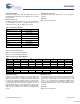
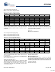
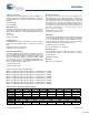
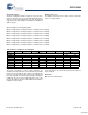
Table Of Contents
- EZ-Host Features
- Typical Applications
- Introduction
- Functional Overview
- Interface Descriptions
- USB Interface
- OTG Interface
- External Memory Interface
- General Purpose IO Interface (GPIO)
- UART Interface
- I2C EEPROM Interface
- Serial Peripheral Interface
- High-Speed Serial Interface
- Programmable Pulse/PWM Interface
- Host Port Interface
- IDE Interface
- Charge Pump Interface
- Booster Interface
- Crystal Interface
- Boot Configuration Interface
- Operational Modes
- Power Savings and Reset Description
- Memory Map
- Registers
- Processor Control Registers
- CPU Flags Register [0xC000] [R]
- Bank Register [0xC002] [R/W]
- Hardware Revision Register [0xC004] [R]
- CPU Speed Register [0xC008] [R/W]
- Power Control Register [0xC00A] [R/W]
- Interrupt Enable Register [0xC00E] [R/W]
- Breakpoint Register [0xC014] [R/W]
- USB Diagnostic Register [0xC03C] [R/W]
- Memory Diagnostic Register [0xC03E] [W]
- External Memory Registers
- Timer Registers
- General USB Registers
- USB Host Only Registers
- Host n Control Register [R/W]
- Host n Address Register [R/W]
- Host n Count Register [R/W]
- Host n Endpoint Status Register [R]
- Host n PID Register [W]
- Host n Count Result Register [R]
- Host n Device Address Register [W]
- Host n Interrupt Enable Register [R/W]
- Host n Status Register [R/W]
- Host n SOF/EOP Count Register [R/W]
- Host n SOF/EOP Counter Register [R]
- Host n Frame Register [R]
- USB Device Only Registers
- Device n Endpoint n Control Register [R/W]
- Device n Endpoint n Address Register [R/W]
- Device n Endpoint n Count Register [R/W]
- Device n Endpoint n Status Register [R/W]
- Device n Endpoint n Count Result Register [R/W]
- Device n Port Select Register [R/W]
- Device n Interrupt Enable Register [R/W]
- Device n Address Register [W]
- Device n Status Register [R/W]
- Device n Frame Number Register [R]
- Device n SOF/EOP Count Register [W]
- OTG Control Registers
- GPIO Registers
- IDE Registers
- HSS Registers
- HSS Control Register [0xC070] [R/W]
- HSS Baud Rate Register [0xC072] [R/W]
- HSS Transmit Gap Register [0xC074] [R/W]
- HSS Data Register [0xC076] [R/W]
- HSS Receive Address Register [0xC078] [R/W]
- HSS Receive Counter Register [0xC07A] [R/W]
- HSS Transmit Address Register [0xC07C] [R/W]
- HSS Transmit Counter Register [0xC07E] [R/W]
- HPI Registers
- SPI Registers
- SPI Configuration Register [0xC0C8] [R/W]
- SPI Control Register [0xC0CA] [R/W]
- SPI Interrupt Enable Register [0xC0CC] [R/W]
- SPI Status Register [0xC0CE] [R]
- SPI Interrupt Clear Register [0xC0D0] [W]
- SPI CRC Control Register [0xC0D2] [R/W]
- SPI CRC Value Register [0xC0D4] [R/W]
- SPI Data Register [0xC0D6] [R/W]
- SPI Transmit Address Register [0xC0D8] [R/W]
- SPI Transmit Count Register [0xC0DA] [R/W]
- SPI Receive Address Register [0xC0DC [R/W]
- SPI Receive Count Register [0xC0DE] [R/W]
- UART Registers
- PWM Registers
- Processor Control Registers
- Pin Diagram
- Pin Descriptions
- Absolute Maximum Ratings
- Operating Conditions
- Crystal Requirements (XTALIN, XTALOUT)
- DC Characteristics
- AC Timing Characteristics
- Register Summary
- Ordering Information
- Package Diagrams
- Document History Page
- Sales, Solutions, and Legal Information
CY7C67300
Document #: 38-08015 Rev. *J Page 34 of 99
Host n Device Address Register [W]
■ Host 1 Device Address Register 0xC088
■ Host 2 Device Address Register 0xC0A8
Register Description
The Host n Device Address register is a write only register that
contains the USB Device Address that the host wants to commu-
nicate with.
Address (Bits [6:0])
The Address field contains the value of the USB address for the
next device that the host is going to communicate with. This
value must be written by firmware.
Reserved
Write all reserved bits with ’0’.
Host n Interrupt Enable Register [R/W]
■ Host 1 Interrupt Enable Register 0xC08C
■ Host 2 Interrupt Enable Register 0xC0AC
Register Description
The Host n Interrupt Enable register enables control over host
related interrupts.
In this register a bit set to ‘1’ enables the corresponding interrupt
while ‘0’ disables the interrupt.
VBUS Interrupt Enable (Bit 15)
The VBUS Interrupt Enable bit enables or disables the OTG
VBUS interrupt. When enabled this interrupt triggers on both the
rising and falling edge of VBUS at the 4.4V status (only
supported in Port 1A). This bit is only available for Host 1 and is
a reserved bit in Host 2.
1: Enable VBUS interrupt
0: Disable VBUS interrupt
ID Interrupt Enable (Bit 14)
The ID Interrupt Enable bit enables or disables the OTG ID
interrupt. When enabled this interrupt triggers on both the rising
and falling edge of the OTG ID pin (only supported in Port 1A).
This bit is only available for Host 1 and is a reserved bit in Host 2.
1: Enable ID interrupt
0: Disable ID interrupt
Table 56. Host n Device Address Register
Bit # 15 14 13 12 11 10 9 8
Field Reserved...
Read/Write - - - - - - - -
Default 0 0 0 0 0 0 0 0
Bit # 7 6 5 4 3 2 1 0
Field ...Reserved Address
Read/Write - W W W W W W W
Default 0 0 0 0 0 0 0 0
Table 57. Host n Interrupt Enable Register
Bit # 15 14 13 12 11 10 9 8
Field
VBUS
Interrupt
Enable
ID Interrupt
Enable
Reserved SOF/EOP
Interrupt
Enable
Reserved
Read/Write R/W R/W - - - - R/W -
Default 0 0 0 0 0 0 0 0
Bit # 7 6 5 4 3 2 1 0
Field
Port B
Wake Interrupt
Enable
Port A
Wake Interrupt
Enable
Port B Connect
Change
Interrupt
Enable
Port A Connect
Change
Interrupt
Enable
Reserved Done
Interrupt
Enable
Read/Write R/W R/W R/W R/W - - - R/W
Default 0 0 0 0 0 0 0 0
[+] Feedback