
Programmable Embedded USB Host and Peripheral Controller with Automotive AEC Grade Support Specification Sheet
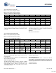
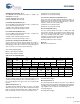
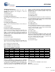
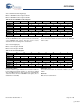
Table Of Contents
- EZ-Host Features
- Typical Applications
- Introduction
- Functional Overview
- Interface Descriptions
- USB Interface
- OTG Interface
- External Memory Interface
- General Purpose IO Interface (GPIO)
- UART Interface
- I2C EEPROM Interface
- Serial Peripheral Interface
- High-Speed Serial Interface
- Programmable Pulse/PWM Interface
- Host Port Interface
- IDE Interface
- Charge Pump Interface
- Booster Interface
- Crystal Interface
- Boot Configuration Interface
- Operational Modes
- Power Savings and Reset Description
- Memory Map
- Registers
- Processor Control Registers
- CPU Flags Register [0xC000] [R]
- Bank Register [0xC002] [R/W]
- Hardware Revision Register [0xC004] [R]
- CPU Speed Register [0xC008] [R/W]
- Power Control Register [0xC00A] [R/W]
- Interrupt Enable Register [0xC00E] [R/W]
- Breakpoint Register [0xC014] [R/W]
- USB Diagnostic Register [0xC03C] [R/W]
- Memory Diagnostic Register [0xC03E] [W]
- External Memory Registers
- Timer Registers
- General USB Registers
- USB Host Only Registers
- Host n Control Register [R/W]
- Host n Address Register [R/W]
- Host n Count Register [R/W]
- Host n Endpoint Status Register [R]
- Host n PID Register [W]
- Host n Count Result Register [R]
- Host n Device Address Register [W]
- Host n Interrupt Enable Register [R/W]
- Host n Status Register [R/W]
- Host n SOF/EOP Count Register [R/W]
- Host n SOF/EOP Counter Register [R]
- Host n Frame Register [R]
- USB Device Only Registers
- Device n Endpoint n Control Register [R/W]
- Device n Endpoint n Address Register [R/W]
- Device n Endpoint n Count Register [R/W]
- Device n Endpoint n Status Register [R/W]
- Device n Endpoint n Count Result Register [R/W]
- Device n Port Select Register [R/W]
- Device n Interrupt Enable Register [R/W]
- Device n Address Register [W]
- Device n Status Register [R/W]
- Device n Frame Number Register [R]
- Device n SOF/EOP Count Register [W]
- OTG Control Registers
- GPIO Registers
- IDE Registers
- HSS Registers
- HSS Control Register [0xC070] [R/W]
- HSS Baud Rate Register [0xC072] [R/W]
- HSS Transmit Gap Register [0xC074] [R/W]
- HSS Data Register [0xC076] [R/W]
- HSS Receive Address Register [0xC078] [R/W]
- HSS Receive Counter Register [0xC07A] [R/W]
- HSS Transmit Address Register [0xC07C] [R/W]
- HSS Transmit Counter Register [0xC07E] [R/W]
- HPI Registers
- SPI Registers
- SPI Configuration Register [0xC0C8] [R/W]
- SPI Control Register [0xC0CA] [R/W]
- SPI Interrupt Enable Register [0xC0CC] [R/W]
- SPI Status Register [0xC0CE] [R]
- SPI Interrupt Clear Register [0xC0D0] [W]
- SPI CRC Control Register [0xC0D2] [R/W]
- SPI CRC Value Register [0xC0D4] [R/W]
- SPI Data Register [0xC0D6] [R/W]
- SPI Transmit Address Register [0xC0D8] [R/W]
- SPI Transmit Count Register [0xC0DA] [R/W]
- SPI Receive Address Register [0xC0DC [R/W]
- SPI Receive Count Register [0xC0DE] [R/W]
- UART Registers
- PWM Registers
- Processor Control Registers
- Pin Diagram
- Pin Descriptions
- Absolute Maximum Ratings
- Operating Conditions
- Crystal Requirements (XTALIN, XTALOUT)
- DC Characteristics
- AC Timing Characteristics
- Register Summary
- Ordering Information
- Package Diagrams
- Document History Page
- Sales, Solutions, and Legal Information
CY7C67300
Document #: 38-08015 Rev. *J Page 32 of 99
Sequence Status (Bit 3)
The Sequence Status bit indicates the state of the last received
data toggle from the device. Firmware is responsible for
monitoring and handling the sequence status. The Sequence bit
is only valid if the ACK bit is set to ‘1’. The Sequence bit is set to
‘0’ when an error is detected in the transaction and the Error bit
is set.
1: DATA1
0: DATA0
Timeout Flag (Bit 2)
The Timeout Flag bit indicates if a timeout condition occurred for
the last transaction. A timeout condition can occur when a device
either takes too long to respond to a USB host request or takes
too long to respond with a handshake.
1: Timeout occurred
0: Timeout did not occur
Error Flag (Bit 1)
The Error Flag bit indicates a transaction failed for any reason
other than the following: timeout, receiving a NAK, or receiving
a STALL. Overflow and Underflow are not considered errors and
do not affect this bit. CRC5 and CRC16 errors result in an Error
flag along with receiving incorrect packet types.
1: Error detected
0: No error detected
ACK Flag (Bit 0)
The ACK Flag bit indicates two different conditions depending on
the transfer type. For non-isochronous transfers, this bit repre-
sents a transaction ending by receiving or sending an ACK
packet. For isochronous transfers, this bit represents a
successful transaction that is not represented by an ACK packet.
1: For non-isochronous transfers, the transaction was ACKed.
For isochronous transfers, the transaction was completed
successfully
0: For non-isochronous transfers, the transaction was not
ACKed. For isochronous transfers, the transaction did not
complete successfully
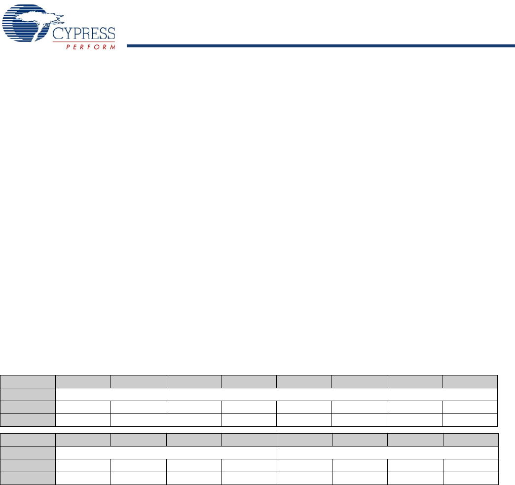
Host n PID Register [W]
■ Host 1 PID Register 0xC086
■ Host 2 PID Register 0xC0A6
Table 53. Host n PID Register
Bit # 15 14 13 12 11 10 9 8
Field Reserved
Read/Write - - - - - - - -
Default 0 0 0 0 0 0 0 0
Bit # 7 6 5 4 3 2 1 0
Field PID Select Endpoint Select
Read/Write W W W W W W W W
Default 0 0 0 0 0 0 0 0
[+] Feedback