
Programmable Embedded USB Host and Peripheral Controller with Automotive AEC Grade Support Specification Sheet
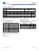
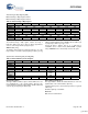
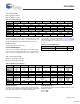
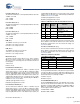
Table Of Contents
- EZ-Host Features
- Typical Applications
- Introduction
- Functional Overview
- Interface Descriptions
- USB Interface
- OTG Interface
- External Memory Interface
- General Purpose IO Interface (GPIO)
- UART Interface
- I2C EEPROM Interface
- Serial Peripheral Interface
- High-Speed Serial Interface
- Programmable Pulse/PWM Interface
- Host Port Interface
- IDE Interface
- Charge Pump Interface
- Booster Interface
- Crystal Interface
- Boot Configuration Interface
- Operational Modes
- Power Savings and Reset Description
- Memory Map
- Registers
- Processor Control Registers
- CPU Flags Register [0xC000] [R]
- Bank Register [0xC002] [R/W]
- Hardware Revision Register [0xC004] [R]
- CPU Speed Register [0xC008] [R/W]
- Power Control Register [0xC00A] [R/W]
- Interrupt Enable Register [0xC00E] [R/W]
- Breakpoint Register [0xC014] [R/W]
- USB Diagnostic Register [0xC03C] [R/W]
- Memory Diagnostic Register [0xC03E] [W]
- External Memory Registers
- Timer Registers
- General USB Registers
- USB Host Only Registers
- Host n Control Register [R/W]
- Host n Address Register [R/W]
- Host n Count Register [R/W]
- Host n Endpoint Status Register [R]
- Host n PID Register [W]
- Host n Count Result Register [R]
- Host n Device Address Register [W]
- Host n Interrupt Enable Register [R/W]
- Host n Status Register [R/W]
- Host n SOF/EOP Count Register [R/W]
- Host n SOF/EOP Counter Register [R]
- Host n Frame Register [R]
- USB Device Only Registers
- Device n Endpoint n Control Register [R/W]
- Device n Endpoint n Address Register [R/W]
- Device n Endpoint n Count Register [R/W]
- Device n Endpoint n Status Register [R/W]
- Device n Endpoint n Count Result Register [R/W]
- Device n Port Select Register [R/W]
- Device n Interrupt Enable Register [R/W]
- Device n Address Register [W]
- Device n Status Register [R/W]
- Device n Frame Number Register [R]
- Device n SOF/EOP Count Register [W]
- OTG Control Registers
- GPIO Registers
- IDE Registers
- HSS Registers
- HSS Control Register [0xC070] [R/W]
- HSS Baud Rate Register [0xC072] [R/W]
- HSS Transmit Gap Register [0xC074] [R/W]
- HSS Data Register [0xC076] [R/W]
- HSS Receive Address Register [0xC078] [R/W]
- HSS Receive Counter Register [0xC07A] [R/W]
- HSS Transmit Address Register [0xC07C] [R/W]
- HSS Transmit Counter Register [0xC07E] [R/W]
- HPI Registers
- SPI Registers
- SPI Configuration Register [0xC0C8] [R/W]
- SPI Control Register [0xC0CA] [R/W]
- SPI Interrupt Enable Register [0xC0CC] [R/W]
- SPI Status Register [0xC0CE] [R]
- SPI Interrupt Clear Register [0xC0D0] [W]
- SPI CRC Control Register [0xC0D2] [R/W]
- SPI CRC Value Register [0xC0D4] [R/W]
- SPI Data Register [0xC0D6] [R/W]
- SPI Transmit Address Register [0xC0D8] [R/W]
- SPI Transmit Count Register [0xC0DA] [R/W]
- SPI Receive Address Register [0xC0DC [R/W]
- SPI Receive Count Register [0xC0DE] [R/W]
- UART Registers
- PWM Registers
- Processor Control Registers
- Pin Diagram
- Pin Descriptions
- Absolute Maximum Ratings
- Operating Conditions
- Crystal Requirements (XTALIN, XTALOUT)
- DC Characteristics
- AC Timing Characteristics
- Register Summary
- Ordering Information
- Package Diagrams
- Document History Page
- Sales, Solutions, and Legal Information
CY7C67300
Document #: 38-08015 Rev. *J Page 30 of 99
Sequence Select (Bit 6)
The Sequence Select bit sets the data toggle for the next packet.
This bit has no effect on receiving data packets; sequence
checking must be handled in firmware.
1: Send DATA1
0: Send DATA0
Sync Enable (Bit 5)
The Sync Enable bit synchronizes the transfer with the SOF
packet in full-speed mode and the EOP packet in low-speed
mode.
1: The next enabled packet is transferred after the SOF or EOP
packet is transmitted
0: The next enabled packet is transferred as soon as the SIE is
free
ISO Enable (Bit 4)
The ISO Enable bit enables or disables an isochronous trans-
action.
1: Enable isochronous transaction
0: Disable isochronous transaction
Arm Enable (Bit 0)
The Arm Enable bit arms an endpoint and starts a transaction.
This bit is automatically cleared to ‘0’ when a transaction is
complete.
1: Arm endpoint and begin transaction
0: Endpoint disarmed
Reserved
Write all reserved bits with ’0’.
Host n Address Register [R/W]
■ Host 1 Address Register 0xC082
■ Host 2 Address Register 0xC0A2
Register Description
The Host n Address register is used as the base pointer into
memory space for the current host transactions.
Address (Bits [15:0])
The Address field sets the address pointer into internal RAM or
ROM.
Host n Count Register [R/W]
■ Host 1 Count Register 0xC084.
■ Host 2 Count Register 0xC0A4.
Table 49. Host n Address Register
Bit # 15 14 13 12 11 10 9 8
Field Address...
Read/Write R/W R/W R/W R/W R/W R/W R/W R/W
Default 0 0 0 0 0 0 0 0
Bit # 7 6 5 4 3 2 1 0
Field ...Address
Read/Write R/W R/W R/W R/W R/W R/W R/W R/W
Default 0 0 0 0 0 0 0 0
Table 50. Host n Count Register
Bit # 15 14 13 12 11 10 9 8
Field
Reserved Port
Select
Reserved Count...
Read/Write - R/W - - - - R/W R/W
Default 0 0 0 0 0 0 0 0
Bit # 7 6 5 4 3 2 1 0
Field ...Count
Read/Write R/W R/W R/W R/W R/W R/W R/W R/W
Default 0 0 0 0 0 0 0 0
[+] Feedback