
Programmable Embedded USB Host and Peripheral Controller with Automotive AEC Grade Support Specification Sheet
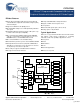
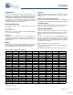
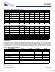
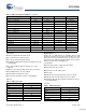
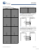
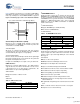
Table Of Contents
- EZ-Host Features
- Typical Applications
- Introduction
- Functional Overview
- Interface Descriptions
- USB Interface
- OTG Interface
- External Memory Interface
- General Purpose IO Interface (GPIO)
- UART Interface
- I2C EEPROM Interface
- Serial Peripheral Interface
- High-Speed Serial Interface
- Programmable Pulse/PWM Interface
- Host Port Interface
- IDE Interface
- Charge Pump Interface
- Booster Interface
- Crystal Interface
- Boot Configuration Interface
- Operational Modes
- Power Savings and Reset Description
- Memory Map
- Registers
- Processor Control Registers
- CPU Flags Register [0xC000] [R]
- Bank Register [0xC002] [R/W]
- Hardware Revision Register [0xC004] [R]
- CPU Speed Register [0xC008] [R/W]
- Power Control Register [0xC00A] [R/W]
- Interrupt Enable Register [0xC00E] [R/W]
- Breakpoint Register [0xC014] [R/W]
- USB Diagnostic Register [0xC03C] [R/W]
- Memory Diagnostic Register [0xC03E] [W]
- External Memory Registers
- Timer Registers
- General USB Registers
- USB Host Only Registers
- Host n Control Register [R/W]
- Host n Address Register [R/W]
- Host n Count Register [R/W]
- Host n Endpoint Status Register [R]
- Host n PID Register [W]
- Host n Count Result Register [R]
- Host n Device Address Register [W]
- Host n Interrupt Enable Register [R/W]
- Host n Status Register [R/W]
- Host n SOF/EOP Count Register [R/W]
- Host n SOF/EOP Counter Register [R]
- Host n Frame Register [R]
- USB Device Only Registers
- Device n Endpoint n Control Register [R/W]
- Device n Endpoint n Address Register [R/W]
- Device n Endpoint n Count Register [R/W]
- Device n Endpoint n Status Register [R/W]
- Device n Endpoint n Count Result Register [R/W]
- Device n Port Select Register [R/W]
- Device n Interrupt Enable Register [R/W]
- Device n Address Register [W]
- Device n Status Register [R/W]
- Device n Frame Number Register [R]
- Device n SOF/EOP Count Register [W]
- OTG Control Registers
- GPIO Registers
- IDE Registers
- HSS Registers
- HSS Control Register [0xC070] [R/W]
- HSS Baud Rate Register [0xC072] [R/W]
- HSS Transmit Gap Register [0xC074] [R/W]
- HSS Data Register [0xC076] [R/W]
- HSS Receive Address Register [0xC078] [R/W]
- HSS Receive Counter Register [0xC07A] [R/W]
- HSS Transmit Address Register [0xC07C] [R/W]
- HSS Transmit Counter Register [0xC07E] [R/W]
- HPI Registers
- SPI Registers
- SPI Configuration Register [0xC0C8] [R/W]
- SPI Control Register [0xC0CA] [R/W]
- SPI Interrupt Enable Register [0xC0CC] [R/W]
- SPI Status Register [0xC0CE] [R]
- SPI Interrupt Clear Register [0xC0D0] [W]
- SPI CRC Control Register [0xC0D2] [R/W]
- SPI CRC Value Register [0xC0D4] [R/W]
- SPI Data Register [0xC0D6] [R/W]
- SPI Transmit Address Register [0xC0D8] [R/W]
- SPI Transmit Count Register [0xC0DA] [R/W]
- SPI Receive Address Register [0xC0DC [R/W]
- SPI Receive Count Register [0xC0DE] [R/W]
- UART Registers
- PWM Registers
- Processor Control Registers
- Pin Diagram
- Pin Descriptions
- Absolute Maximum Ratings
- Operating Conditions
- Crystal Requirements (XTALIN, XTALOUT)
- DC Characteristics
- AC Timing Characteristics
- Register Summary
- Ordering Information
- Package Diagrams
- Document History Page
- Sales, Solutions, and Legal Information

CY7C67300
Document #: 38-08015 Rev. *J Page 3 of 99
USB Interface
EZ-Host has two built in Host/Peripheral SIEs and four USB transceivers that meet the USB 2.0 specification requirements for full and
low speed (high speed is not supported). In Host mode, EZ-Host supports four downstream ports, each support control, interrupt, bulk,
and isochronous transfers. In Peripheral mode, EZ-Host supports one peripheral port with eight endpoints for each of the two SIEs.
Endpoint 0 is dedicated as the control endpoint and only supports control transfers. Endpoints 1 though 7 support interrupt, bulk (up
to 64 bytes/packet), or isochronous transfers (up to 1023 Bytes/packet size). EZ-Host also supports a combination of Host and
Peripheral ports simultaneously as shown in Table 3.
GPIO10 D10 D10 SCK
[1]
GPIO9 D9 D9 nSSI
[1]
GPIO8 D8 D8 MISO
[1]
GPIO7 D7 D7
GPIO6 D6 D6
GPIO5 D5 D5
GPIO4 D4 D4
GPIO3 D3 D3
GPIO2 D2 D2
GPIO1 D1 D1
GPIO0 D0 D0
Table 1. Interface Options for GPIO Pins (continued)
GPIO Pins HPI IDE PWM HSS SPI UART I2C OTG
Note
2. Alternate interface location.
Table 2. Interface Options for External Memory Bus Pins
MEM Pins HPI IDE PWM HSS SPI UART I2C OTG
D15 CTS
[2]
D14 RTS
[2]
D13 RXD
[2]
D12 TXD
[2]
D11 MOSI
[2]
D10 SCK
[2]
D9 nSSI
[2]
D8 MISO
[2]
D[7:0]
A[18:0]
CONTROL
Table 3. USB Port Configuration Options
Port Configurations Port 1A Port 1B Port 2A Port 2B
OTG OTG – – –
OTG + 2 Hosts OTG – Host Host
OTG + 1 Host OTG – Host –
OTG + 1 Host OTG – – Host
OTG + 1 Peripheral OTG – Peripheral –
OTG + 1 Peripheral OTG – – Peripheral
4 Hosts Host Host Host Host
3 Hosts Any Combination of Ports
2 Hosts Any Combination of Ports
1 Host Any Port
[+] Feedback