
Programmable Embedded USB Host and Peripheral Controller with Automotive AEC Grade Support Specification Sheet
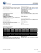
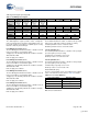
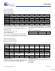
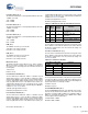
Table Of Contents
- EZ-Host Features
- Typical Applications
- Introduction
- Functional Overview
- Interface Descriptions
- USB Interface
- OTG Interface
- External Memory Interface
- General Purpose IO Interface (GPIO)
- UART Interface
- I2C EEPROM Interface
- Serial Peripheral Interface
- High-Speed Serial Interface
- Programmable Pulse/PWM Interface
- Host Port Interface
- IDE Interface
- Charge Pump Interface
- Booster Interface
- Crystal Interface
- Boot Configuration Interface
- Operational Modes
- Power Savings and Reset Description
- Memory Map
- Registers
- Processor Control Registers
- CPU Flags Register [0xC000] [R]
- Bank Register [0xC002] [R/W]
- Hardware Revision Register [0xC004] [R]
- CPU Speed Register [0xC008] [R/W]
- Power Control Register [0xC00A] [R/W]
- Interrupt Enable Register [0xC00E] [R/W]
- Breakpoint Register [0xC014] [R/W]
- USB Diagnostic Register [0xC03C] [R/W]
- Memory Diagnostic Register [0xC03E] [W]
- External Memory Registers
- Timer Registers
- General USB Registers
- USB Host Only Registers
- Host n Control Register [R/W]
- Host n Address Register [R/W]
- Host n Count Register [R/W]
- Host n Endpoint Status Register [R]
- Host n PID Register [W]
- Host n Count Result Register [R]
- Host n Device Address Register [W]
- Host n Interrupt Enable Register [R/W]
- Host n Status Register [R/W]
- Host n SOF/EOP Count Register [R/W]
- Host n SOF/EOP Counter Register [R]
- Host n Frame Register [R]
- USB Device Only Registers
- Device n Endpoint n Control Register [R/W]
- Device n Endpoint n Address Register [R/W]
- Device n Endpoint n Count Register [R/W]
- Device n Endpoint n Status Register [R/W]
- Device n Endpoint n Count Result Register [R/W]
- Device n Port Select Register [R/W]
- Device n Interrupt Enable Register [R/W]
- Device n Address Register [W]
- Device n Status Register [R/W]
- Device n Frame Number Register [R]
- Device n SOF/EOP Count Register [W]
- OTG Control Registers
- GPIO Registers
- IDE Registers
- HSS Registers
- HSS Control Register [0xC070] [R/W]
- HSS Baud Rate Register [0xC072] [R/W]
- HSS Transmit Gap Register [0xC074] [R/W]
- HSS Data Register [0xC076] [R/W]
- HSS Receive Address Register [0xC078] [R/W]
- HSS Receive Counter Register [0xC07A] [R/W]
- HSS Transmit Address Register [0xC07C] [R/W]
- HSS Transmit Counter Register [0xC07E] [R/W]
- HPI Registers
- SPI Registers
- SPI Configuration Register [0xC0C8] [R/W]
- SPI Control Register [0xC0CA] [R/W]
- SPI Interrupt Enable Register [0xC0CC] [R/W]
- SPI Status Register [0xC0CE] [R]
- SPI Interrupt Clear Register [0xC0D0] [W]
- SPI CRC Control Register [0xC0D2] [R/W]
- SPI CRC Value Register [0xC0D4] [R/W]
- SPI Data Register [0xC0D6] [R/W]
- SPI Transmit Address Register [0xC0D8] [R/W]
- SPI Transmit Count Register [0xC0DA] [R/W]
- SPI Receive Address Register [0xC0DC [R/W]
- SPI Receive Count Register [0xC0DE] [R/W]
- UART Registers
- PWM Registers
- Processor Control Registers
- Pin Diagram
- Pin Descriptions
- Absolute Maximum Ratings
- Operating Conditions
- Crystal Requirements (XTALIN, XTALOUT)
- DC Characteristics
- AC Timing Characteristics
- Register Summary
- Ordering Information
- Package Diagrams
- Document History Page
- Sales, Solutions, and Legal Information
CY7C67300
Document #: 38-08015 Rev. *J Page 28 of 99
Port B D– Status (Bit 14)
The Port B D– Status bit is a read only bit that indicates the value
of DATA– on Port B.
1: D– is HIGH
0: D– is LOW
Port A D+ Status (Bit 13)
The Port A D+ Status bit is a read only bit that indicates the value
of DATA+ on Port A.
1: D+ is HIGH
0: D+ is LOW
Port A D– Status (Bit 12)
The Port A D– Status bit is a read only bit that indicates the value
of DATA– on Port A.
1: D– is HIGH
0: D– is LOW
LOB (Bit 11)
The LOB bit selects the speed of Port B.
1: Port B is set to low-speed mode
0: Port B is set to full-speed mode
LOA (Bit 10)
The LOA bit selects the speed of Port A.
1: Port A is set to low-speed mode
0: Port A is set to full-speed mode
Mode Select (Bit 9)
The Mode Select bit sets the SIE for host or device operation.
When set for device operation only one USB port is supported.
The active port is selected by the Port Select bit in the Host n
Count register.
1: Host mode
0: Device mode
Port B Resistors Enable (Bit 8)
The Port B Resistors Enable bit enables or disables the pull
up/pull down resistors on Port B. When enabled, the Mode
Select bit and LOB bit of this register set the pull up/pull down
resistors appropriately. When the Mode Select is set for Host
mode, the pull down resistors on the data lines (D+ and D–) are
enabled. When the Mode Select is set for Device mode, a single
pull up resistor on either D+ or D–, determined by the LOB bit, is
enabled. See Table 45 for details.
1: Enable pull up/pull down resistors
0: Disable pull up/pull down resistors
Port A Resistors Enable (Bit 7)
The Port A Resistors Enable bit enables or disables the pull
up/pull down resistors on Port A. When enabled, the Mode
Select bit and LOA bit of this register set the pull up/pull down
resistors appropriately. When the Mode Select is set for Host
mode, the pull down resistors on the data lines (D+ and D–) are
enabled. When the Mode Select is set for Device mode, a single
pull up resistor on either D+ or D–, determined by the LOA bit, is
enabled. See Table 45 for details.
1: Enable pull up/pull down resistors
0: Disable pull up/pull down resistors
Port B Force D± State (Bits [6:5])
The Port B Force D± State field controls the forcing state of the
D+ D– data lines for Port B. This field forces the state of the Port
B data lines independent of the Port Select bit setting. See
Table 46 for details.
Port A Force D± State (Bits [4:3])
The Port A Force D± State field controls the forcing state of the
D+ D– data lines for Port A. This field forces the state of the Port
A data lines independent of the Port Select bit setting. See
Table 46 for details.
Suspend Enable (Bit 2)
The Suspend Enable bit enables or disables the suspend feature
on both ports. When suspend is enabled the USB transceivers
are powered down and cannot transmit or received USB packets
but can still monitor for a wakeup condition.
1: Enable suspend
0: Disable suspend
Port B SOF/EOP Enable (Bit 1)
The Port B SOF/EOP Enable bit is only applicable in host mode.
In device mode, this bit must be written as ‘0’. In host mode this
bit enables or disables SOFs or EOPs for Port B. Either SOFs or
EOPs are generated depending on the LOB bit in the USB n
Control register when Port B is active.
1: Enable SOFs or EOPs
0: Disable SOFs or EOPs
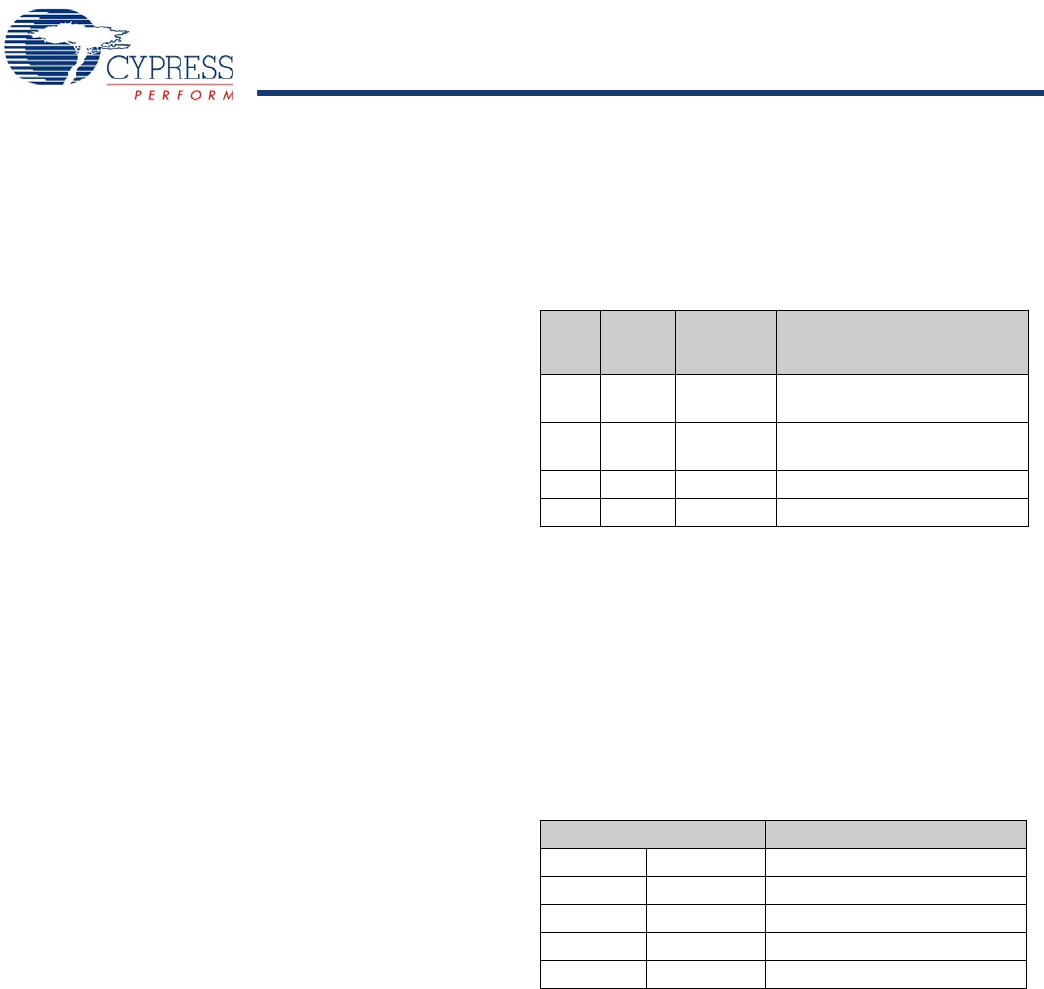
Table 45. USB Data Line Pull Up and Pull Down Resistors
L0A/
L0B
Mode
Select
Port n
Resistors
Enable
Function
X X 0 Pull up/Pull down on D+ and
D– Disabled
X 1 1 Pull down on D+ and
D– Enabled
1 0 1 Pull up on USB D– Enabled
0 0 1 Pull up on USB D+ Enabled
Table 46. Port A/B Force D± State
Port A/B Force D± State Function
MSb LSb
0 0 Normal Operation
1 0 Force USB Reset, SE0 State
0 1 Force J-State
1 1 Force K-State
[+] Feedback