
Programmable Embedded USB Host and Peripheral Controller with Automotive AEC Grade Support Specification Sheet
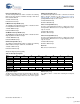
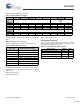
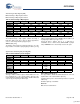
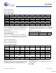
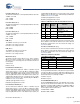
Table Of Contents
- EZ-Host Features
- Typical Applications
- Introduction
- Functional Overview
- Interface Descriptions
- USB Interface
- OTG Interface
- External Memory Interface
- General Purpose IO Interface (GPIO)
- UART Interface
- I2C EEPROM Interface
- Serial Peripheral Interface
- High-Speed Serial Interface
- Programmable Pulse/PWM Interface
- Host Port Interface
- IDE Interface
- Charge Pump Interface
- Booster Interface
- Crystal Interface
- Boot Configuration Interface
- Operational Modes
- Power Savings and Reset Description
- Memory Map
- Registers
- Processor Control Registers
- CPU Flags Register [0xC000] [R]
- Bank Register [0xC002] [R/W]
- Hardware Revision Register [0xC004] [R]
- CPU Speed Register [0xC008] [R/W]
- Power Control Register [0xC00A] [R/W]
- Interrupt Enable Register [0xC00E] [R/W]
- Breakpoint Register [0xC014] [R/W]
- USB Diagnostic Register [0xC03C] [R/W]
- Memory Diagnostic Register [0xC03E] [W]
- External Memory Registers
- Timer Registers
- General USB Registers
- USB Host Only Registers
- Host n Control Register [R/W]
- Host n Address Register [R/W]
- Host n Count Register [R/W]
- Host n Endpoint Status Register [R]
- Host n PID Register [W]
- Host n Count Result Register [R]
- Host n Device Address Register [W]
- Host n Interrupt Enable Register [R/W]
- Host n Status Register [R/W]
- Host n SOF/EOP Count Register [R/W]
- Host n SOF/EOP Counter Register [R]
- Host n Frame Register [R]
- USB Device Only Registers
- Device n Endpoint n Control Register [R/W]
- Device n Endpoint n Address Register [R/W]
- Device n Endpoint n Count Register [R/W]
- Device n Endpoint n Status Register [R/W]
- Device n Endpoint n Count Result Register [R/W]
- Device n Port Select Register [R/W]
- Device n Interrupt Enable Register [R/W]
- Device n Address Register [W]
- Device n Status Register [R/W]
- Device n Frame Number Register [R]
- Device n SOF/EOP Count Register [W]
- OTG Control Registers
- GPIO Registers
- IDE Registers
- HSS Registers
- HSS Control Register [0xC070] [R/W]
- HSS Baud Rate Register [0xC072] [R/W]
- HSS Transmit Gap Register [0xC074] [R/W]
- HSS Data Register [0xC076] [R/W]
- HSS Receive Address Register [0xC078] [R/W]
- HSS Receive Counter Register [0xC07A] [R/W]
- HSS Transmit Address Register [0xC07C] [R/W]
- HSS Transmit Counter Register [0xC07E] [R/W]
- HPI Registers
- SPI Registers
- SPI Configuration Register [0xC0C8] [R/W]
- SPI Control Register [0xC0CA] [R/W]
- SPI Interrupt Enable Register [0xC0CC] [R/W]
- SPI Status Register [0xC0CE] [R]
- SPI Interrupt Clear Register [0xC0D0] [W]
- SPI CRC Control Register [0xC0D2] [R/W]
- SPI CRC Value Register [0xC0D4] [R/W]
- SPI Data Register [0xC0D6] [R/W]
- SPI Transmit Address Register [0xC0D8] [R/W]
- SPI Transmit Count Register [0xC0DA] [R/W]
- SPI Receive Address Register [0xC0DC [R/W]
- SPI Receive Count Register [0xC0DE] [R/W]
- UART Registers
- PWM Registers
- Processor Control Registers
- Pin Diagram
- Pin Descriptions
- Absolute Maximum Ratings
- Operating Conditions
- Crystal Requirements (XTALIN, XTALOUT)
- DC Characteristics
- AC Timing Characteristics
- Register Summary
- Ordering Information
- Package Diagrams
- Document History Page
- Sales, Solutions, and Legal Information
CY7C67300
Document #: 38-08015 Rev. *J Page 25 of 99
External Memory Control Register [0xC03A] [R/W]
Register Description
The External Memory Control register provides control of Wait
States for the external SRAM or ROM. All wait states are based
off of 48 MHz.
XRAM Merge Enable (Bit 13)
The XRAM Merge Enable bit enables or disables the RAM merge
feature. When the RAM merge feature is enabled, the
nXRAMSEL is active whenever the nXMEMSEL is active.
1: Enable RAM merge
0: Disable RAM merge
XROM Merge Enable (Bit 12)
The XROM Merge Enable bit enables or disables the ROM
merge feature. When the ROM merge feature is enabled, the
nXROMSEL is active whenever the nXMEMSEL is active.
1: Enable ROM merge
0: Disable ROM merge
XMEM Width Select (Bit 11)
The XMEM Width Select bit selects the extended memory width.
1: Extended memory = 8
0: Extended memory = 16
XMEM Wait Select (Bits [10:8])
The XMEM Wait Select field selects the extended memory wait
state from 0 to 7.
XROM Width Select (Bit 7)
The XROM Width Select bit selects the external ROM width.
1: External memory = 8
0: External memory = 16
XROM Wait Select (Bits[6:4])
The XROM Wait Select field selects the external ROM wait state
from 0 to 7.
XRAM Width Select (Bit 3)
The XRAM Width Select bit selects the external RAM width.
1: External memory = 8
0: External memory = 16
XRAM Wait Select (Bits[2:0])
The XRAM Wait Select field selects the external RAM wait state
from 0 to 7.
Reserved
Write all reserved bits with ’0’.
Timer Registers
There are three registers dedicated to timer operations. Each of
these registers are discussed in this section and are summarized
in Table 39.
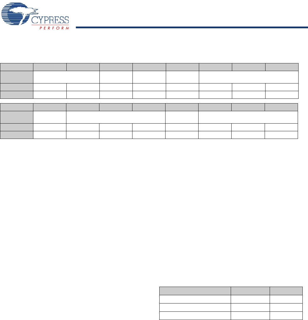
Table 38. External Memory Control Register
Bit # 15 14 13 12 11 10 9 8
Field
Reserved XRAM Merge
Enable
XROM Merge
Enable
XMEM Width
Select
XMEM Wait
Select
Read/Write - - R/W R/W R/W R/W R/W R/W
Default X X X X X X X X
Bit # 7 6 5 4 3 2 1 0
Field
XROM Width
Select
XROM Wait
Select
XRAM Width
Select
XRAM Wait
Select
Read/Write R/W R/W R/W R/W R/W R/W R/W R/W
Default X X X X X X X X
Table 39. Timer Registers
Register Name Address R/W
Watchdog Timer Register 0xC00C R/W
Timer 0 Register 0xC010 R/W
Timer 1 Register 0xC012 R/W
[+] Feedback