
Programmable Embedded USB Host and Peripheral Controller with Automotive AEC Grade Support Specification Sheet
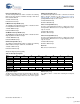
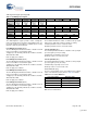
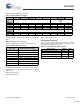
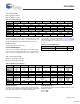
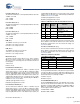
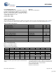
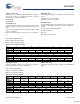
Table Of Contents
- EZ-Host Features
- Typical Applications
- Introduction
- Functional Overview
- Interface Descriptions
- USB Interface
- OTG Interface
- External Memory Interface
- General Purpose IO Interface (GPIO)
- UART Interface
- I2C EEPROM Interface
- Serial Peripheral Interface
- High-Speed Serial Interface
- Programmable Pulse/PWM Interface
- Host Port Interface
- IDE Interface
- Charge Pump Interface
- Booster Interface
- Crystal Interface
- Boot Configuration Interface
- Operational Modes
- Power Savings and Reset Description
- Memory Map
- Registers
- Processor Control Registers
- CPU Flags Register [0xC000] [R]
- Bank Register [0xC002] [R/W]
- Hardware Revision Register [0xC004] [R]
- CPU Speed Register [0xC008] [R/W]
- Power Control Register [0xC00A] [R/W]
- Interrupt Enable Register [0xC00E] [R/W]
- Breakpoint Register [0xC014] [R/W]
- USB Diagnostic Register [0xC03C] [R/W]
- Memory Diagnostic Register [0xC03E] [W]
- External Memory Registers
- Timer Registers
- General USB Registers
- USB Host Only Registers
- Host n Control Register [R/W]
- Host n Address Register [R/W]
- Host n Count Register [R/W]
- Host n Endpoint Status Register [R]
- Host n PID Register [W]
- Host n Count Result Register [R]
- Host n Device Address Register [W]
- Host n Interrupt Enable Register [R/W]
- Host n Status Register [R/W]
- Host n SOF/EOP Count Register [R/W]
- Host n SOF/EOP Counter Register [R]
- Host n Frame Register [R]
- USB Device Only Registers
- Device n Endpoint n Control Register [R/W]
- Device n Endpoint n Address Register [R/W]
- Device n Endpoint n Count Register [R/W]
- Device n Endpoint n Status Register [R/W]
- Device n Endpoint n Count Result Register [R/W]
- Device n Port Select Register [R/W]
- Device n Interrupt Enable Register [R/W]
- Device n Address Register [W]
- Device n Status Register [R/W]
- Device n Frame Number Register [R]
- Device n SOF/EOP Count Register [W]
- OTG Control Registers
- GPIO Registers
- IDE Registers
- HSS Registers
- HSS Control Register [0xC070] [R/W]
- HSS Baud Rate Register [0xC072] [R/W]
- HSS Transmit Gap Register [0xC074] [R/W]
- HSS Data Register [0xC076] [R/W]
- HSS Receive Address Register [0xC078] [R/W]
- HSS Receive Counter Register [0xC07A] [R/W]
- HSS Transmit Address Register [0xC07C] [R/W]
- HSS Transmit Counter Register [0xC07E] [R/W]
- HPI Registers
- SPI Registers
- SPI Configuration Register [0xC0C8] [R/W]
- SPI Control Register [0xC0CA] [R/W]
- SPI Interrupt Enable Register [0xC0CC] [R/W]
- SPI Status Register [0xC0CE] [R]
- SPI Interrupt Clear Register [0xC0D0] [W]
- SPI CRC Control Register [0xC0D2] [R/W]
- SPI CRC Value Register [0xC0D4] [R/W]
- SPI Data Register [0xC0D6] [R/W]
- SPI Transmit Address Register [0xC0D8] [R/W]
- SPI Transmit Count Register [0xC0DA] [R/W]
- SPI Receive Address Register [0xC0DC [R/W]
- SPI Receive Count Register [0xC0DE] [R/W]
- UART Registers
- PWM Registers
- Processor Control Registers
- Pin Diagram
- Pin Descriptions
- Absolute Maximum Ratings
- Operating Conditions
- Crystal Requirements (XTALIN, XTALOUT)
- DC Characteristics
- AC Timing Characteristics
- Register Summary
- Ordering Information
- Package Diagrams
- Document History Page
- Sales, Solutions, and Legal Information
CY7C67300
Document #: 38-08015 Rev. *J Page 22 of 99
USB Diagnostic Register [0xC03C] [R/W]
Register Description
The USB Diagnostic register provides control of diagnostic
modes. It is intended for use by device characterization tests, not
for normal operations. This register is read/write by the on-chip
CPU but is write-only via the HPI port.
Port 2B Diagnostic Enable (Bit 15)
The Port 2B Diagnostic Enable bit enables or disables Port 2B
for the test conditions selected in this register.
1: Apply any of the following enabled test conditions: J/K, DCK,
SE0, RSF, RSL, PRD
0: Do not apply test conditions
Port 2A Diagnostic Enable (Bit 14)
The Port 2A Diagnostic Enable bit enables or disables Port 2A
for the test conditions selected in this register.
1: Apply any of the following enabled test conditions: J/K, DCK,
SE0, RSF, RSL, PRD
0: Do not apply test conditions
Port 1B Diagnostic Enable (Bit 13)
The Port 1B Diagnostic Enable bit enables or disables Port 1B
for the test conditions selected in this register.
1: Apply any of the following enabled test conditions: J/K, DCK,
SE0, RSF, RSL, PRD
0: Do not apply test conditions
Port 1A Diagnostic Enable (Bit 12)
The Port 1A Diagnostic Enable bit enables or disables Port 1A
for the test conditions selected in this register.
1: Apply any of the following enabled test conditions: J/K, DCK,
SE0, RSF, RSL, PRD
0: Do not apply test conditions
Pull-down Enable (Bit 6)
The Pull-down Enable bit enables or disables full-speed pull
down resistors (pull down on both D+ and D–) for testing.
1: Enable pull down resistors on both D+ and D–
0: Disable pull down resistors on both D+ and D–
LS Pull-up Enable (Bit 5)
The LS Pull-up Enable bit enables or disables a low-speed pull
up resistor (pull up on D–) for testing.
1: Enable low-speed pull up resistor on D–
0: Pull-up resistor is not connected on D–
FS Pull-up Enable (Bit 4)
The FS Pull-up Enable bit enables or disables a full-speed pull
up resistor (pull up on D+) for testing.
1: Enable full-speed pull up resistor on D+
0: Pull up resistor is not connected on D+
Force Select (Bits [2:0])
The Force Select field bit selects several different test condition
states on the data lines (D+/D–). Refer to Table 32 for details.
Reserved
Write all reserved bits with ’0’.
Table 31. USB Diagnostic Register
Bit # 15 14 13 12 11 10 9 8
Field
Port 2B
Diagnostic
Enable
Port 2A
Diagnostic
Enable
Port 1B
Diagnostic
Enable
Port 1A
Diagnostic
Enable
Reserved...
Read/Write R/W R/W R/W R/W - - - -
Default 0 0 0 0 0 0 0 0
Bit # 7 6 5 4 3 2 1 0
Field
...Reserved Pull-down
Enable
LS Pull-up
Enable
FS Pull-up
Enable
Reserved Force Select
Read/Write - R/W R/W R/W - R/W R/W R/W
Default 0 0 0 0 0 0 0 0
Table 32. Force Select Definition
Force Select [2:0] Data Line State
1xx Assert SE0
01x Toggle JK
001 Assert J
000 Assert K
[+] Feedback