
Programmable Embedded USB Host and Peripheral Controller with Automotive AEC Grade Support Specification Sheet
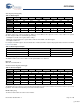
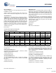
Table Of Contents
- EZ-Host Features
- Typical Applications
- Introduction
- Functional Overview
- Interface Descriptions
- USB Interface
- OTG Interface
- External Memory Interface
- General Purpose IO Interface (GPIO)
- UART Interface
- I2C EEPROM Interface
- Serial Peripheral Interface
- High-Speed Serial Interface
- Programmable Pulse/PWM Interface
- Host Port Interface
- IDE Interface
- Charge Pump Interface
- Booster Interface
- Crystal Interface
- Boot Configuration Interface
- Operational Modes
- Power Savings and Reset Description
- Memory Map
- Registers
- Processor Control Registers
- CPU Flags Register [0xC000] [R]
- Bank Register [0xC002] [R/W]
- Hardware Revision Register [0xC004] [R]
- CPU Speed Register [0xC008] [R/W]
- Power Control Register [0xC00A] [R/W]
- Interrupt Enable Register [0xC00E] [R/W]
- Breakpoint Register [0xC014] [R/W]
- USB Diagnostic Register [0xC03C] [R/W]
- Memory Diagnostic Register [0xC03E] [W]
- External Memory Registers
- Timer Registers
- General USB Registers
- USB Host Only Registers
- Host n Control Register [R/W]
- Host n Address Register [R/W]
- Host n Count Register [R/W]
- Host n Endpoint Status Register [R]
- Host n PID Register [W]
- Host n Count Result Register [R]
- Host n Device Address Register [W]
- Host n Interrupt Enable Register [R/W]
- Host n Status Register [R/W]
- Host n SOF/EOP Count Register [R/W]
- Host n SOF/EOP Counter Register [R]
- Host n Frame Register [R]
- USB Device Only Registers
- Device n Endpoint n Control Register [R/W]
- Device n Endpoint n Address Register [R/W]
- Device n Endpoint n Count Register [R/W]
- Device n Endpoint n Status Register [R/W]
- Device n Endpoint n Count Result Register [R/W]
- Device n Port Select Register [R/W]
- Device n Interrupt Enable Register [R/W]
- Device n Address Register [W]
- Device n Status Register [R/W]
- Device n Frame Number Register [R]
- Device n SOF/EOP Count Register [W]
- OTG Control Registers
- GPIO Registers
- IDE Registers
- HSS Registers
- HSS Control Register [0xC070] [R/W]
- HSS Baud Rate Register [0xC072] [R/W]
- HSS Transmit Gap Register [0xC074] [R/W]
- HSS Data Register [0xC076] [R/W]
- HSS Receive Address Register [0xC078] [R/W]
- HSS Receive Counter Register [0xC07A] [R/W]
- HSS Transmit Address Register [0xC07C] [R/W]
- HSS Transmit Counter Register [0xC07E] [R/W]
- HPI Registers
- SPI Registers
- SPI Configuration Register [0xC0C8] [R/W]
- SPI Control Register [0xC0CA] [R/W]
- SPI Interrupt Enable Register [0xC0CC] [R/W]
- SPI Status Register [0xC0CE] [R]
- SPI Interrupt Clear Register [0xC0D0] [W]
- SPI CRC Control Register [0xC0D2] [R/W]
- SPI CRC Value Register [0xC0D4] [R/W]
- SPI Data Register [0xC0D6] [R/W]
- SPI Transmit Address Register [0xC0D8] [R/W]
- SPI Transmit Count Register [0xC0DA] [R/W]
- SPI Receive Address Register [0xC0DC [R/W]
- SPI Receive Count Register [0xC0DE] [R/W]
- UART Registers
- PWM Registers
- Processor Control Registers
- Pin Diagram
- Pin Descriptions
- Absolute Maximum Ratings
- Operating Conditions
- Crystal Requirements (XTALIN, XTALOUT)
- DC Characteristics
- AC Timing Characteristics
- Register Summary
- Ordering Information
- Package Diagrams
- Document History Page
- Sales, Solutions, and Legal Information

CY7C67300
Document #: 38-08015 Rev. *J Page 20 of 99
Boost 3V OK (Bit 2)
The Boost 3V OK bit is a read only bit that returns the status of
the OTG Boost circuit.
1: Boost circuit not ok and internal voltage rails are below 3.0V
0: Boost circuit ok and internal voltage rails are at or above 3.0V
Sleep Enable (Bit 1)
Setting this bit to ‘1’ immediately initiates SLEEP mode. While in
SLEEP mode, the entire chip is paused, achieving the lowest
standby power state. All operations are paused, the internal
clock is stopped, the booster circuit and OTG VBUS charge
pump are all powered down, and the USB transceivers are
powered down. All counters and timers are paused but retain
their values; enabled PWM outputs freeze in their current states.
SLEEP mode exits by any activity selected in this register. When
SLEEP mode ends, instruction execution resumes within 0.5 ms.
1: Enable Sleep mode
0: No function
Halt Enable (Bit 0)
Setting this bit to ‘1’ immediately initiates HALT mode. While in
HALT mode, only the CPU is stopped. The internal clock still runs
and all peripherals still operate, including the USB engines. The
power saving using HALT in most cases is minimal, but in appli-
cations that are very CPU intensive the incremental savings may
provide some benefit.
The HALT state is exited when any enabled interrupt is triggered.
Upon exiting the HALT state, one or two instructions immediately
following the HALT instruction may be executed before the
waking interrupt is serviced (you may want to follow the HALT
instruction with two NOPs).
1: Enable Halt mode
0: No function
Reserved
Write all reserved bits with ’0’.
Interrupt Enable Register [0xC00E] [R/W]
Register Description
The Interrupt Enable register allows control of the hardware
interrupt vectors.
OTG Interrupt Enable (Bit 12)
The OTG Interrupt Enable bit enables or disables the OTG
ID/OTG4.4V Valid hardware interrupt.
1: Enable OTG interrupt
0: Disable OTG interrupt
SPI Interrupt Enable (Bit 11)
The SPI Interrupt Enable bit enables or disables the following
three SPI hardware interrupts: SPI TX, SPI RX, and SPI DMA
Block Done.
1: Enable SPI interrupt
0: Disable SPI interrupt
Host/Device 2 Interrupt Enable (Bit 9)
The Host/Device 2 Interrupt Enable bit enables or disables all of
the following Host/Device 2 hardware interrupts: Host 2 USB
Done, Host 2 USB SOF/EOP, Host 2 Wakeup/Insert/Remove,
Device 2 Reset, Device 2 SOF/EOP or WakeUp from USB,
Device 2 Endpoint n.
1: Enable Host 2 and Device 2 interrupt
0: Disable Host 2 and Device 2 interrupt
Host/Device 1 Interrupt Enable (Bit 8)
The Host/Device 1 Interrupt Enable bit enables or disables all of
the following Host/Device 1 hardware interrupts: Host 1 USB
Done, Host 1 USB SOF/EOP, Host 1 Wakeup/Insert/Remove,
Device 1 Reset, Device 1 SOF/EOP or WakeUp from USB,
Device 1Endpoint n.
1: Enable Host 1 and Device 1 interrupt
0: Disable Host 1 and Device 1 interrupt
Table 29. Interrupt Enable Register
Bit # 15 14 13 12 11 10 9 8
Field
Reserved OTG
Interrupt
Enable
SPI
Interrupt
Enable
Reserved Host/Device 2
Interrupt
Enable
Host/Device 1
Interrupt
Enable
Read/Write - - - R/W R/W - R/W R/W
Default 0 0 0 0 0 0 0 0
Bit # 7 6 5 4 3 2 1 0
Field
HSS
Interrupt
Enable
In Mailbox
Interrupt
Enable
Out Mailbox
Interrupt
Enable
Reserved UART
Interrupt
Enable
GPIO
Interrupt
Enable
Timer 1
Interrupt
Enable
Timer 0
Interrupt
Enable
Read/Write R/W R/W R/W - R/W R/W R/W R/W
Default 0 0 0 1 0 0 0 0
[+] Feedback