
Programmable Embedded USB Host and Peripheral Controller with Automotive AEC Grade Support Specification Sheet
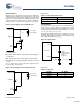
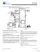
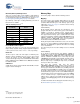
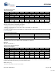
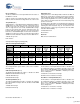
Table Of Contents
- EZ-Host Features
- Typical Applications
- Introduction
- Functional Overview
- Interface Descriptions
- USB Interface
- OTG Interface
- External Memory Interface
- General Purpose IO Interface (GPIO)
- UART Interface
- I2C EEPROM Interface
- Serial Peripheral Interface
- High-Speed Serial Interface
- Programmable Pulse/PWM Interface
- Host Port Interface
- IDE Interface
- Charge Pump Interface
- Booster Interface
- Crystal Interface
- Boot Configuration Interface
- Operational Modes
- Power Savings and Reset Description
- Memory Map
- Registers
- Processor Control Registers
- CPU Flags Register [0xC000] [R]
- Bank Register [0xC002] [R/W]
- Hardware Revision Register [0xC004] [R]
- CPU Speed Register [0xC008] [R/W]
- Power Control Register [0xC00A] [R/W]
- Interrupt Enable Register [0xC00E] [R/W]
- Breakpoint Register [0xC014] [R/W]
- USB Diagnostic Register [0xC03C] [R/W]
- Memory Diagnostic Register [0xC03E] [W]
- External Memory Registers
- Timer Registers
- General USB Registers
- USB Host Only Registers
- Host n Control Register [R/W]
- Host n Address Register [R/W]
- Host n Count Register [R/W]
- Host n Endpoint Status Register [R]
- Host n PID Register [W]
- Host n Count Result Register [R]
- Host n Device Address Register [W]
- Host n Interrupt Enable Register [R/W]
- Host n Status Register [R/W]
- Host n SOF/EOP Count Register [R/W]
- Host n SOF/EOP Counter Register [R]
- Host n Frame Register [R]
- USB Device Only Registers
- Device n Endpoint n Control Register [R/W]
- Device n Endpoint n Address Register [R/W]
- Device n Endpoint n Count Register [R/W]
- Device n Endpoint n Status Register [R/W]
- Device n Endpoint n Count Result Register [R/W]
- Device n Port Select Register [R/W]
- Device n Interrupt Enable Register [R/W]
- Device n Address Register [W]
- Device n Status Register [R/W]
- Device n Frame Number Register [R]
- Device n SOF/EOP Count Register [W]
- OTG Control Registers
- GPIO Registers
- IDE Registers
- HSS Registers
- HSS Control Register [0xC070] [R/W]
- HSS Baud Rate Register [0xC072] [R/W]
- HSS Transmit Gap Register [0xC074] [R/W]
- HSS Data Register [0xC076] [R/W]
- HSS Receive Address Register [0xC078] [R/W]
- HSS Receive Counter Register [0xC07A] [R/W]
- HSS Transmit Address Register [0xC07C] [R/W]
- HSS Transmit Counter Register [0xC07E] [R/W]
- HPI Registers
- SPI Registers
- SPI Configuration Register [0xC0C8] [R/W]
- SPI Control Register [0xC0CA] [R/W]
- SPI Interrupt Enable Register [0xC0CC] [R/W]
- SPI Status Register [0xC0CE] [R]
- SPI Interrupt Clear Register [0xC0D0] [W]
- SPI CRC Control Register [0xC0D2] [R/W]
- SPI CRC Value Register [0xC0D4] [R/W]
- SPI Data Register [0xC0D6] [R/W]
- SPI Transmit Address Register [0xC0D8] [R/W]
- SPI Transmit Count Register [0xC0DA] [R/W]
- SPI Receive Address Register [0xC0DC [R/W]
- SPI Receive Count Register [0xC0DE] [R/W]
- UART Registers
- PWM Registers
- Processor Control Registers
- Pin Diagram
- Pin Descriptions
- Absolute Maximum Ratings
- Operating Conditions
- Crystal Requirements (XTALIN, XTALOUT)
- DC Characteristics
- AC Timing Characteristics
- Register Summary
- Ordering Information
- Package Diagrams
- Document History Page
- Sales, Solutions, and Legal Information

CY7C67300
Document #: 38-08015 Rev. *J Page 19 of 99
Power Control Register [0xC00A] [R/W]
Register Description
The Power Control register controls the power down and wakeup
options. Either the sleep mode or the halt mode options can be
selected. All other writable bits in this register can be used as a
wakeup source while in sleep mode.
Host/Device 2B Wake Enable (Bit 15)
The Host/Device 2B Wake Enable bit enables or disables a
wakeup condition to occur on a Host/Device 2B transition. This
wakeup from the SIE port does not cause an interrupt to the
on-chip CPU.
1: Enable wakeup on Host/Device 2B transition
0: Disable wakeup on Host/Device 2B transition
Host/Device 2A Wake Enable (Bit 14)
The Host/Device 2A Wake Enable bit enables or disables a
wakeup condition to occur on an Host/Device 2A transition. This
wakeup from the SIE port does not cause an interrupt to the
on-chip CPU.
1: Enable wakeup on Host/Device 2A transition
0: Disable wakeup on Host/Device 2A transition
Host/Device 1B Wake Enable (Bit 13)
The Host/Device 1B Wake Enable bit enables or disables a
wakeup condition to occur on an Host/Device 1B transition. This
wakeup from the SIE port does not cause an interrupt to the
on-chip CPU.
1: Enable wakeup on Host/Device 1B transition
0: Disable wakeup on Host/Device 1B transition
Host/Device 1A Wake Enable (Bit 12)
The Host/Device 1A Wake Enable bit enables or disables a
wakeup condition to occur on an Host/Device 1A transition. This
wakeup from the SIE port does not cause an interrupt to the
on-chip CPU.
1: Enable wakeup on Host/Device 1A transition
0: Disable wakeup on Host/Device 1A transition
OTG Wake Enable (Bit 11)
The OTG Wake Enable bit enables or disables a wakeup
condition to occur on either an OTG VBUS_Valid or OTG ID
transition (IRQ20).
1: Enable wakeup on OTG VBUS valid or OTG ID transition
0: Disable wakeup on OTG VBUS valid or OTG ID transition
HSS Wake Enable (Bit 9)
The HSS Wake Enable bit enables or disables a wakeup
condition to occur on an HSS Rx serial input transition. The
processor may take several hundreds of microseconds before
being operational after wakeup. Therefore, the incoming data
byte that causes the wakeup is discarded.
1: Enable wakeup on HSS Rx serial input transition
0: Disable wakeup on HSS Rx serial input transition
SPI Wake Enable (Bit 8)
The SPI Wake Enable bit enables or disables a wakeup condition
to occur on a falling SPI_nSS input transition. The processor
may take several hundreds of microseconds before being opera-
tional after wakeup. Therefore, the incoming data byte that
causes the wakeup is discarded.
1: Enable wakeup on falling SPI nSS input transition
0: Disable SPI_nSS interrupt
HPI Wake Enable (Bit 7)
The HPI Wake Enable bit enables or disables a wakeup
condition to occur on an HPI interface read.
1: Enable wakeup on HPI interface read
0: Disable wakeup on HPI interface read
GPI Wake Enable (Bit 4)
The GPI Wake Enable bit enables or disables a wakeup
condition to occur on a GPIO(25:24) transition.
1: Enable wakeup on GPIO(25:24) transition
0: Disable wakeup on GPIO(25:24) transition
Table 28. Power Control Register
Bit # 15 14 13 12 11 10 9 8
Field
Host/Device
2B
Wake
Enable
Host/Device
2A
Wake
Enable
Host/Device
1B
Wake
Enable
Host/Device
1A
Wake
Enable
OTG
Wake
Enable
Reserved HSS
Wake
Enable
SPI
Wake
Enable
Read/Write R/W R/W R/W R/W R/W - R/W R/W
Default 0 0 0 0 0 0 0 0
Bit # 7 6 5 4 3 2 1 0
Field
HPI
Wake
Enable
Reserved GPI
Wake
Enable
Reserved Boost 3V
OK
Sleep
Enable
Halt
Enable
Read/Write R/W - - R/W - R R/W R/W
Default 0 0 0 0 0 0 0 0
[+] Feedback