
Programmable Embedded USB Host and Peripheral Controller with Automotive AEC Grade Support Specification Sheet
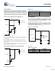
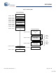
Table Of Contents
- EZ-Host Features
- Typical Applications
- Introduction
- Functional Overview
- Interface Descriptions
- USB Interface
- OTG Interface
- External Memory Interface
- General Purpose IO Interface (GPIO)
- UART Interface
- I2C EEPROM Interface
- Serial Peripheral Interface
- High-Speed Serial Interface
- Programmable Pulse/PWM Interface
- Host Port Interface
- IDE Interface
- Charge Pump Interface
- Booster Interface
- Crystal Interface
- Boot Configuration Interface
- Operational Modes
- Power Savings and Reset Description
- Memory Map
- Registers
- Processor Control Registers
- CPU Flags Register [0xC000] [R]
- Bank Register [0xC002] [R/W]
- Hardware Revision Register [0xC004] [R]
- CPU Speed Register [0xC008] [R/W]
- Power Control Register [0xC00A] [R/W]
- Interrupt Enable Register [0xC00E] [R/W]
- Breakpoint Register [0xC014] [R/W]
- USB Diagnostic Register [0xC03C] [R/W]
- Memory Diagnostic Register [0xC03E] [W]
- External Memory Registers
- Timer Registers
- General USB Registers
- USB Host Only Registers
- Host n Control Register [R/W]
- Host n Address Register [R/W]
- Host n Count Register [R/W]
- Host n Endpoint Status Register [R]
- Host n PID Register [W]
- Host n Count Result Register [R]
- Host n Device Address Register [W]
- Host n Interrupt Enable Register [R/W]
- Host n Status Register [R/W]
- Host n SOF/EOP Count Register [R/W]
- Host n SOF/EOP Counter Register [R]
- Host n Frame Register [R]
- USB Device Only Registers
- Device n Endpoint n Control Register [R/W]
- Device n Endpoint n Address Register [R/W]
- Device n Endpoint n Count Register [R/W]
- Device n Endpoint n Status Register [R/W]
- Device n Endpoint n Count Result Register [R/W]
- Device n Port Select Register [R/W]
- Device n Interrupt Enable Register [R/W]
- Device n Address Register [W]
- Device n Status Register [R/W]
- Device n Frame Number Register [R]
- Device n SOF/EOP Count Register [W]
- OTG Control Registers
- GPIO Registers
- IDE Registers
- HSS Registers
- HSS Control Register [0xC070] [R/W]
- HSS Baud Rate Register [0xC072] [R/W]
- HSS Transmit Gap Register [0xC074] [R/W]
- HSS Data Register [0xC076] [R/W]
- HSS Receive Address Register [0xC078] [R/W]
- HSS Receive Counter Register [0xC07A] [R/W]
- HSS Transmit Address Register [0xC07C] [R/W]
- HSS Transmit Counter Register [0xC07E] [R/W]
- HPI Registers
- SPI Registers
- SPI Configuration Register [0xC0C8] [R/W]
- SPI Control Register [0xC0CA] [R/W]
- SPI Interrupt Enable Register [0xC0CC] [R/W]
- SPI Status Register [0xC0CE] [R]
- SPI Interrupt Clear Register [0xC0D0] [W]
- SPI CRC Control Register [0xC0D2] [R/W]
- SPI CRC Value Register [0xC0D4] [R/W]
- SPI Data Register [0xC0D6] [R/W]
- SPI Transmit Address Register [0xC0D8] [R/W]
- SPI Transmit Count Register [0xC0DA] [R/W]
- SPI Receive Address Register [0xC0DC [R/W]
- SPI Receive Count Register [0xC0DE] [R/W]
- UART Registers
- PWM Registers
- Processor Control Registers
- Pin Diagram
- Pin Descriptions
- Absolute Maximum Ratings
- Operating Conditions
- Crystal Requirements (XTALIN, XTALOUT)
- DC Characteristics
- AC Timing Characteristics
- Register Summary
- Ordering Information
- Package Diagrams
- Document History Page
- Sales, Solutions, and Legal Information
CY7C67300
Document #: 38-08015 Rev. *J Page 13 of 99
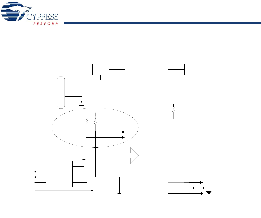
Minimum Hardware Requirements for Standalone Mode – Peripheral Only
Power Savings and Reset Description
This sections describes the different modes for resetting the chip
and ways to save power.
Power Saving Mode Description
EZ-Host has one main power saving mode, Sleep. For detailed
information about Sleep mode, see the Sleep section that
follows.
Sleep mode is used for USB applications to support USB
suspend and non USB applications as the main chip power down
mode.
In addition, EZ-Host is capable of slowing down the CPU clock
speed through the CPU Speed register [0xC008] without
affecting other peripheral timing. Reducing the CPU clock speed
from 48 MHz to 24 MHz reduces the overall current draw by
around 8 mA while reducing it from 48 MHz to 3 MHz reduces
the overall current draw by approximately 15 mA.
Sleep
Sleep mode is the main chip power down mode and is also used
for USB suspend. Sleep mode is entered by setting the Sleep
Enable (bit 1) of the Power control register [0xC00A]. During
Sleep mode (USB Suspend) the following events and states are
true:
■ GPIO pins maintain their configuration during sleep (in
suspend)
■ External Memory address pins are driven low
■ XTALOUT is turned off
■ Internal PLL is turned off
■ Ensure that firmware disables the charge pump (OTG Control
register [0xC098]) thereby causing OTGVBUS to drop below
0.2V. Otherwise OTGVBUS only drops to V
CC
– (2 schottky
diode drops).
■ Booster circuit is turned off
■ USB transceivers is turned off
■ CPU goes into suspend mode until a programmable wakeup
event
Figure 9. Minimum Standalone Hardware Configuration – Peripheral Only
EZ-Host
CY7C67300
GPIO[30]
GPIO[31]
SCL*
SDA*
10k
Bootstrap Options
Bootloading Firmware
*Bootloading begins after POR + 3ms BIOS bootup
Vcc
10k
Vcc
A2
GND
A0
A1
SCL
SDA
VCC
WP
VCC
Up to 64k x8
EEPROM
*GPIO[31:30] 31 30
Up to 2k x8 SCL SDA
>2k x8 to 64k x8 SDA SCL
Int. 16k x8
Code / Data
XOUT
XIN
12MHz
22pf
22pf
nRESET
Reset
Logic
*
Parallel Resonant
Fundamental Mode
500uW
20-33pf ±5%
VCC, AVCC,
BoostVCC
VReg
DMinus
DPlus
Standard-B
or Mini-B
D+
VBus
GND
D-
SHIELD
Reserved
GND, AGND,
BoostGND
Pin 38
VCC
47Kohm
[+] Feedback