
Programmable Embedded USB Host and Peripheral Controller with Automotive AEC Grade Support Specification Sheet
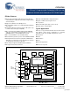
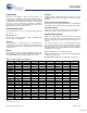
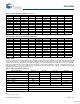
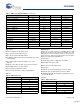
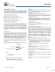
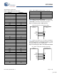
Table Of Contents
- EZ-Host Features
- Typical Applications
- Introduction
- Functional Overview
- Interface Descriptions
- USB Interface
- OTG Interface
- External Memory Interface
- General Purpose IO Interface (GPIO)
- UART Interface
- I2C EEPROM Interface
- Serial Peripheral Interface
- High-Speed Serial Interface
- Programmable Pulse/PWM Interface
- Host Port Interface
- IDE Interface
- Charge Pump Interface
- Booster Interface
- Crystal Interface
- Boot Configuration Interface
- Operational Modes
- Power Savings and Reset Description
- Memory Map
- Registers
- Processor Control Registers
- CPU Flags Register [0xC000] [R]
- Bank Register [0xC002] [R/W]
- Hardware Revision Register [0xC004] [R]
- CPU Speed Register [0xC008] [R/W]
- Power Control Register [0xC00A] [R/W]
- Interrupt Enable Register [0xC00E] [R/W]
- Breakpoint Register [0xC014] [R/W]
- USB Diagnostic Register [0xC03C] [R/W]
- Memory Diagnostic Register [0xC03E] [W]
- External Memory Registers
- Timer Registers
- General USB Registers
- USB Host Only Registers
- Host n Control Register [R/W]
- Host n Address Register [R/W]
- Host n Count Register [R/W]
- Host n Endpoint Status Register [R]
- Host n PID Register [W]
- Host n Count Result Register [R]
- Host n Device Address Register [W]
- Host n Interrupt Enable Register [R/W]
- Host n Status Register [R/W]
- Host n SOF/EOP Count Register [R/W]
- Host n SOF/EOP Counter Register [R]
- Host n Frame Register [R]
- USB Device Only Registers
- Device n Endpoint n Control Register [R/W]
- Device n Endpoint n Address Register [R/W]
- Device n Endpoint n Count Register [R/W]
- Device n Endpoint n Status Register [R/W]
- Device n Endpoint n Count Result Register [R/W]
- Device n Port Select Register [R/W]
- Device n Interrupt Enable Register [R/W]
- Device n Address Register [W]
- Device n Status Register [R/W]
- Device n Frame Number Register [R]
- Device n SOF/EOP Count Register [W]
- OTG Control Registers
- GPIO Registers
- IDE Registers
- HSS Registers
- HSS Control Register [0xC070] [R/W]
- HSS Baud Rate Register [0xC072] [R/W]
- HSS Transmit Gap Register [0xC074] [R/W]
- HSS Data Register [0xC076] [R/W]
- HSS Receive Address Register [0xC078] [R/W]
- HSS Receive Counter Register [0xC07A] [R/W]
- HSS Transmit Address Register [0xC07C] [R/W]
- HSS Transmit Counter Register [0xC07E] [R/W]
- HPI Registers
- SPI Registers
- SPI Configuration Register [0xC0C8] [R/W]
- SPI Control Register [0xC0CA] [R/W]
- SPI Interrupt Enable Register [0xC0CC] [R/W]
- SPI Status Register [0xC0CE] [R]
- SPI Interrupt Clear Register [0xC0D0] [W]
- SPI CRC Control Register [0xC0D2] [R/W]
- SPI CRC Value Register [0xC0D4] [R/W]
- SPI Data Register [0xC0D6] [R/W]
- SPI Transmit Address Register [0xC0D8] [R/W]
- SPI Transmit Count Register [0xC0DA] [R/W]
- SPI Receive Address Register [0xC0DC [R/W]
- SPI Receive Count Register [0xC0DE] [R/W]
- UART Registers
- PWM Registers
- Processor Control Registers
- Pin Diagram
- Pin Descriptions
- Absolute Maximum Ratings
- Operating Conditions
- Crystal Requirements (XTALIN, XTALOUT)
- DC Characteristics
- AC Timing Characteristics
- Register Summary
- Ordering Information
- Package Diagrams
- Document History Page
- Sales, Solutions, and Legal Information
CY7C67300
Document #: 38-08015 Rev. *J Page 10 of 99
IDE Features
■ Programmable IO mode 0–4
■ Block mode transfers
■ Direct memory access to/from internal memory through the IDE
data register
IDE Pins
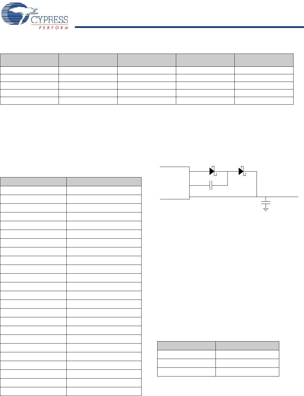
Charge Pump Interface
VBUS for the USB OTG port can be produced by EZ-Host using
its built in charge pump and some external components. Ensure
the circuit connections look similar to the following diagram.
Component details:
■ D1 and D2: Schottky diodes with a current rating greater than
60 mA
■ C1: Ceramic capacitor with a capacitance of 0.1 µF
■ C2: Make capacitor value no more that 6.5 µF since that is the
maximum capacitance allowed by the USB OTG specifications
for a dual role device. The minimum value of C2 is 1 µF. There
are no restrictions on the type of capacitor for C2.
If the VBUS charge pump circuit is not to be used, CSWITCHA,
CSWITCHB, and OTGVBUS can be left unconnected.
Charge Pump Features
■ Meets OTG Supplement Requirements, see Table 134, DC
Characteristics: Charge Pump on page 84 for details.
Charge Pump Pins
Table 14. IDE Throughput
Mode
ATA/ATAPI-4
Min Cycle Time
Actual
Min Cycle Time
ATA/ATPI-4
Max Transfer Rate
Actual
Max Transfer Rate
PIO Mode 0 600 ns 30T = 625 ns 3.33 MB/s 3.2 MB/s
PIO Mode 1 383 ns 20T = 416.7 ns 5.22 MB/s 4.8 MB/s
PIO Mode 2 240 13T = 270.8 ns 8.33 MB/s 7.38 MB/s
PIO Mode 3 180 ns 10T = 208.3 ns 11.11 MB/s 9.6 MB/s
PIO Mode 4 120 ns 8T = 166.7 ns 16.67 MB/s 12.0 MB/s
T = System clock period = 1/48 MHz.
Table 15. IDE Interface Pins
Pin Name Pin Number
IORDY 46
IOR 47
IOW 48
CS1 50
CS0 52
A2 53
A1 54
A0 55
D15 56
D14 57
D13 58
D12 59
D11 60
D10 61
D9 65
D8 66
D7 86
D6 87
D5 89
D4 90
D3 91
D2 92
D1 93
D0 94
Figure 5. Charge Pump
Table 16. Charge Pump Interface Pins
Pin Name Pin Number
OTGVBUS 11
CSwitchA 13
CSwitchB 12
VBUS
D1
D2
C1
C2
CSWITCHA
CSWITCHB
OTGVBUS
CY7C67300
[+] Feedback