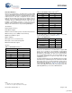
CY7C67300 EZ-Host™ Programmable Embedded USB Host and Peripheral Controller with Automotive AEC Grade Support EZ-Host Features ■ Single chip programmable USB dual-role (Host/Peripheral) controller with two configurable Serial Interface Engines (SIEs) and four USB ports ■ Support for USB On-The-Go (OTG) protocol ■ On-chip 48 MHz 16-bit processor with dynamically switchable clock speed ■ On-chip 16-bit DMA/mailbox data path interface ■ Supports 12 MHz external crystal or clock ■ 3.
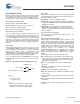
CY7C67300 Introduction Interrupts EZ-Host™ (CY7C67300) is Cypress Semiconductor’s first full-speed, low cost multiport host/peripheral controller. EZ-Host is designed to easily interface to most high performance CPUs to add USB host functionality. EZ-Host has its own 16-bit RISC processor to act as a coprocessor or operate in standalone mode. EZ-Host also has a programmable IO interface block allowing a wide range of interface options. EZ-Host provides 128 interrupt vectors.
CY7C67300 Table 1. Interface Options for GPIO Pins (continued) GPIO Pins GPIO10 GPIO9 GPIO8 GPIO7 GPIO6 GPIO5 GPIO4 GPIO3 GPIO2 GPIO1 GPIO0 HPI D10 D9 D8 D7 D6 D5 D4 D3 D2 D1 D0 IDE D10 D9 D8 D7 D6 D5 D4 D3 D2 D1 D0 PWM HSS SPI SCK[1] nSSI[1] MISO[1] UART I2C OTG HSS CTS[2] RTS[2] RXD[2] TXD[2] SPI UART I2C OTG Table 2.
CY7C67300 Table 3.
CY7C67300 External Memory Interface Merge Mode EZ-Host provides a robust interface to a wide variety of external memory arrays. All available external memory array locations can contain either code or data. The CY16 RISC processor directly addresses a flat memory space from 0x0000 to 0xFFFF.
CY7C67300 External Memory Interface Pins Table 6. External Memory Interface Pins (continued) Table 6. External Memory Interface Pins Pin Name Pin Number Pin Name Pin Number D3 80 nWR 64 D2 81 nRD 62 D1 82 nXMEMSEL (optional nCS) 34 D0 83 nXROMSEL (ROM nCS) 35 nXRAMSEL (RAM nCS) 36 External Memory Interface Block Diagrams A18 95 A17 96 Figure 2 illustrates how to connect a 64k × 8 memory array (SRAM/ROM) to the EZ-Host external memory interface.
CY7C67300 Figure 4 illustrates the interface for connecting an 8-bit ROM or 8-bit RAM to the EZ-Host external memory interface. In 8-bit mode, up to 512K bytes of external ROM or RAM are supported. Figure 4. Interfacing up to 512k × 8 for External Code/Data Up to 512k x 8 External Code/Data (Page Mode) EZ-Host CY7C67300 External Memory Array Up to 512k x8 I2C EEPROM Interface EZ-Host provides a master-only I2C interface for external serial EEPROMs.
CY7C67300 SPI Pins HSS Pins The SPI port has a few different pin location options as shown in Table 9. The port location is selectable via the GPIO control register [0xC006]. The HSS port has a few different pin location options as shown in Table 10. The port location is selectable via the GPIO control register [0xC006]. Table 9. SPI Interface Pins Table 10.
CY7C67300 Table 12. HPI Interface Pins (continued)[3, 4] Host Port Interface EZ-Host has an HPI interface. The HPI interface provides DMA access to the EZ-Host internal memory by an external host, plus a bidirectional mailbox register for supporting high level communication protocols. This port is designed to be the primary high-speed connection to a host processor. Complete control of EZ-Host can be accomplished through this interface via an extensible API and communication protocol.
CY7C67300 Table 14. IDE Throughput ATA/ATAPI-4 Min Cycle Time PIO Mode 0 600 ns PIO Mode 1 383 ns PIO Mode 2 240 PIO Mode 3 180 ns PIO Mode 4 120 ns T = System clock period = 1/48 MHz. Mode Actual Min Cycle Time 30T = 625 ns 20T = 416.7 ns 13T = 270.8 ns 10T = 208.3 ns 8T = 166.7 ns ATA/ATPI-4 Max Transfer Rate 3.33 MB/s 5.22 MB/s 8.33 MB/s 11.11 MB/s 16.67 MB/s Actual Max Transfer Rate 3.2 MB/s 4.8 MB/s 7.38 MB/s 9.6 MB/s 12.
CY7C67300 Booster Interface Booster Pins EZ-Host has an on chip power booster circuit for use with power supplies that range between 2.7V and 3.6V. The booster circuit boosts the power to 3.3V nominal to supply power for the entire chip. The booster circuit requires an external inductor, diode, and capacitor. During power down mode, the circuit is disabled to save power. Figure 6 shows how to connect the booster circuit. Table 17. Charge Pump Interface Pins Figure 6.
CY7C67300 Boot Configuration Interface Operational Modes EZ-Host can boot into any one of four modes. The mode it boots into is determined by the TTL voltage level of GPIO[31:30] at the time nRESET is deasserted. Table 19 shows the different boot pin combinations possible. After a reset pin event occurs, the BIOS bootup procedure executes for up to 3 ms. GPIO[31:30] are sampled by the BIOS during bootup only. After bootup these pins are available to the application as GPIOs.
CY7C67300 Minimum Hardware Requirements for Standalone Mode – Peripheral Only Figure 9. Minimum Standalone Hardware Configuration – Peripheral Only EZ-Host CY7C67300 VCC, AVCC, BoostVCC VReg Standard-B or Mini-B VBus D+ Reset Logic nRESET DPlus DMinus DGND SHIELD VCC Bootstrap Options 47Kohm Vcc Vcc Pin 38 10k 10k GPIO[30] SCL* GPIO[31] SDA* Int.
CY7C67300 External (Remote) Wakeup Source There are several possible events available to wake EZ-Host from Sleep mode as shown in Table 20. These may also be used as remote wakeup options for USB applications. See the Power Control Register [0xC00A] [R/W] on page 19 for details. Upon wakeup, code begins executing within 200 µs, the time it takes the PLL to stabilize. Table 20.
CY7C67300 Figure 10. Memory Map Internal Memory HW INT's 0x0000 - 0x00FF SW INT's 0x0100 - 0x011F 0x0120 - 0x013F 0x0140 - 0x0148 0x014A - 0x01FF Primary Registers Swap Registers HPI Int / Mailbox LCP Variables 0x0200 - 0x02FF USB Registers 0x0300 - 0x030F 0x0310 - 0x03FF 0x0400 - 0x04A2 Slave Setup Packet BIOS Stack USB Slave & OTG 0x04A4 - 0x3FFF USER SPACE ~15K 0xC000 - 0xC0FF 0xE000 - 0xFFFF Document #: 38-08015 Rev.
CY7C67300 Registers Table 21. Processor Control Registers Some registers have different functions for a read vs. a write access or USB host vs. USB device mode. Therefore, registers of this type have multiple definitions for the same address. CPU Flags Register Register Name The default register values listed in this data sheet may be altered to some other value during the BIOS initialization. Refer to the BIOS documentation for register initialization information.
CY7C67300 Bank Register [0xC002] [R/W] Table 23. Bank Register Bit # 15 14 13 12 11 10 9 8 R/W R/W R/W R/W Default 0 0 R/W R/W R/W R/W 0 0 0 0 0 1 Bit # 7 6 5 4 3 2 1 0 Field Read/Write Address... Field Read/Write Default ...Address Reserved R/W R/W R/W - - - - - 0 0 0 X X X X X Register Description The Bank register maps registers R0–R15 into RAM. The eleven MSBs of this register are used as a base address for registers R0–R15.
CY7C67300 CPU Speed Register [0xC008] [R/W] Table 26. CPU Speed Register Bit # 15 14 13 12 Read/Write - - - - - - - - Default 0 0 0 0 0 0 0 0 Bit # 7 6 5 4 3 2 1 0 Read/Write - - - - R/W R/W R/W R/W Default 0 0 0 0 1 1 1 1 Field 11 10 9 8 Reserved... Field ...Reserved CPU Speed Register Description The CPU Speed register allows the processor to operate at a user selected speed.
CY7C67300 Power Control Register [0xC00A] [R/W] Table 28.
CY7C67300 Boost 3V OK (Bit 2) Halt Enable (Bit 0) The Boost 3V OK bit is a read only bit that returns the status of the OTG Boost circuit. Setting this bit to ‘1’ immediately initiates HALT mode. While in HALT mode, only the CPU is stopped. The internal clock still runs and all peripherals still operate, including the USB engines. The power saving using HALT in most cases is minimal, but in applications that are very CPU intensive the incremental savings may provide some benefit.
CY7C67300 HSS Interrupt Enable (Bit 7) GPIO Interrupt Enable (Bit 2) The HSS Interrupt Enable bit enables or disables the following High-speed Serial Interface hardware interrupts: HSS Block Done and HSS RX Full. 1: Enable HSS interrupt The GPIO Interrupt Enable bit enables or disables the General Purpose IO pins interrupt (see the GPIO Control Register [0xC006] [R/W] on page 50).
CY7C67300 USB Diagnostic Register [0xC03C] [R/W] Table 31. USB Diagnostic Register Bit # 15 14 13 12 Field Port 2B Diagnostic Enable Port 2A Diagnostic Enable Port 1B Diagnostic Enable Port 1A Diagnostic Enable Read/Write 11 10 9 8 Reserved... R/W R/W R/W R/W - - - - Default 0 0 0 0 0 0 0 0 Bit # 7 6 5 4 3 2 1 0 ...
CY7C67300 Memory Diagnostic Register [0xC03E] [W] Table 33. Memory Diagnostic Register Bit # 15 14 13 12 11 10 Reserved 9 8 Memory Arbitration Select Field Read/Write - - - - - W W W Default 0 0 0 0 0 0 0 0 Bit # 7 6 5 4 3 2 1 0 Reserved Monitor Enable Field Read/Write - - - - - - - W Default 0 0 0 0 0 0 0 0 Register Description Reserved The Memory Diagnostic register provides control of diagnostic modes. Write all reserved bits with ’0’.
CY7C67300 Extended Page n Map Register [R/W] ■ Extended Page 1 Map Register 0xC018 ■ Extended Page 2 Map Register 0xC01A Table 36. Extended Page n Map Register Bit # 15 14 13 12 11 10 9 8 R/W R/W R/W R/W Default 0 0 R/W R/W R/W R/W 0 0 0 0 0 0 Bit # 7 6 5 4 3 2 1 0 R/W R/W R/W R/W R/W R/W R/W R/W 0 0 0 0 0 0 0 0 Field Read/Write Address... Field Read/Write Default ...
CY7C67300 External Memory Control Register [0xC03A] [R/W] Table 38.
CY7C67300 Watchdog Timer Register [0xC00C] [R/W] Table 40. Watchdog Timer Register Bit # 15 14 13 12 11 10 9 8 R/W R/W R/W R/W Default 0 0 R/W R/W R/W R/W 0 0 0 0 0 0 Bit # 7 6 5 4 3 2 1 0 Lock Enable WDT Enable Reset Strobe Field Reserved... Read/Write ...
CY7C67300 Timer n Register [R/W] ■ Timer 0 Register 0xC010 ■ Timer 1 Register 0xC012 Table 42. Timer n Register Bit # 15 14 13 12 11 10 9 8 R/W R/W R/W R/W Default 1 1 R/W R/W R/W R/W 1 1 1 1 1 1 Bit # 7 6 5 4 3 2 1 0 R/W R/W R/W R/W R/W R/W R/W R/W 1 1 1 1 1 1 1 1 Field Count... Read/Write Field ...Count Read/Write Default Register Description The Timer n Register sets the Timer n count.
CY7C67300 The Port B D– Status bit is a read only bit that indicates the value of DATA– on Port B. enabled. When the Mode Select is set for Device mode, a single pull up resistor on either D+ or D–, determined by the LOA bit, is enabled. See Table 45 for details. 1: D– is HIGH 1: Enable pull up/pull down resistors 0: D– is LOW 0: Disable pull up/pull down resistors Port B D– Status (Bit 14) Port A D+ Status (Bit 13) Table 45.
CY7C67300 Port A SOF/EOP Enable (Bit 0) Reserved The Port A SOF/EOP Enable bit is only applicable in host mode. In device mode this bit must be written as ‘0’. In host mode this bit enables or disables SOFs or EOPs for Port A. Either SOFs or EOPs are generated depending on the LOA bit in the USB n Control register when Port A is active. Write all reserved bits with ’0’.
CY7C67300 Sequence Select (Bit 6) ISO Enable (Bit 4) The Sequence Select bit sets the data toggle for the next packet. This bit has no effect on receiving data packets; sequence checking must be handled in firmware. The ISO Enable bit enables or disables an isochronous transaction.
CY7C67300 Register Description Table 51. Port Select Definition The Host n Count register is used to hold the number of bytes (packet length) for the current transaction. The maximum packet length is 1023 bytes in ISO mode. The Host Count value is used to determine how many bytes to transmit, or the maximum number of bytes to receive. If the number of received bytes is greater then the Host Count value then an overflow condition is flagged by the Overflow bit in the Host n Endpoint Status register.
CY7C67300 Sequence Status (Bit 3) The Sequence Status bit indicates the state of the last received data toggle from the device. Firmware is responsible for monitoring and handling the sequence status. The Sequence bit is only valid if the ACK bit is set to ‘1’. The Sequence bit is set to ‘0’ when an error is detected in the transaction and the Error bit is set. 1: DATA1 0: DATA0 Timeout Flag (Bit 2) The Timeout Flag bit indicates if a timeout condition occurred for the last transaction.
CY7C67300 Register Description Endpoint Select (Bits [3:0]) The Host n PID register is a write only register that provides the PID and Endpoint information to the USB SIE to be used in the next transaction. The Endpoint field allows addressing of up to 16 different endpoints. PID Select (Bits [7:4]) Write all reserved bits with ’0’. Reserved The PID Select field is defined in Table 54.
CY7C67300 Host n Device Address Register [W] ■ Host 1 Device Address Register 0xC088 ■ Host 2 Device Address Register 0xC0A8 Table 56. Host n Device Address Register Bit # 15 14 13 12 Read/Write - - - - - - - - Default 0 0 0 0 0 0 0 0 Bit # 7 6 5 4 3 2 1 0 Field ...Reserved Field 11 10 9 8 Reserved...
CY7C67300 SOF/EOP Interrupt Enable (Bit 9) 1: Enable Connect Change interrupt The SOF/EOP Interrupt Enable bit enables or disables the SOF/EOP timer interrupt 0: Disable Connect Change interrupt Port A Connect Change Interrupt Enable (Bit 4) 1: Enable SOF/EOP timer interrupt The Port A Connect Change Interrupt Enable bit enables or disables the Connect Change interrupt on Port A.
CY7C67300 The SOF/EOP Interrupt Flag bit indicates the status of the SOF/EOP Timer interrupt. This bit triggers ‘1’ when the SOF/EOP timer expires. triggers ‘1’ on either a rising edge or falling edge of a USB Reset condition (device inserted or removed). Together with the Port A SE0 Status bit, it can be determined whether a device was inserted or removed.
CY7C67300 Host n SOF/EOP Counter Register [R] ■ Host 1 SOF/EOP Counter Register 0xC094 ■ Host 2 SOF/EOP Counter Register 0xC0B4 Table 60. Host n SOF/EOP Counter Register Bit # 15 Field 14 13 12 11 Reserved 10 9 8 Counter... Read/Write - - R R R R R R Default X X X X X X X X Bit # 7 6 5 4 3 2 1 0 Read/Write R R R R R R R R Default X X X X X X X X Field ...
CY7C67300 USB Device Only Registers There are eleven sets of USB Device Only registers. All sets consist of at least two registers, one for Device Port 1 and one for Device Port 2. In addition, each Device port has eight possible endpoints. This gives each endpoint register set eight registers for each Device Port for a total of sixteen registers per set. The USB Device Only registers are covered in this section and summarized in Table 62. Table 62.
CY7C67300 Sequence Select (Bit 6) Direction Select (Bit 2) The Sequence Select bit determines whether a DATA0 or a DATA1 is sent for the next data toggle. This bit has no effect on receiving data packets; sequence checking must be handled in firmware. 1: Send a DATA1 0: Send a DATA0 The Direction Select bit needs to be set according to the expected direction of the next data stage in the next transaction.
CY7C67300 Register Description Address (Bits [15:0]) The Device n Endpoint n Address register is used as the base pointer into memory space for the current Endpoint transaction. There are a total of eight endpoints for each of the two ports. All endpoints have the same definition for their Device n Endpoint n Address register. The Address field sets the base address for the current transaction on a signal endpoint.
CY7C67300 Device n Endpoint n Status Register [R/W] ■ Device n Endpoint 0 Status Register [Device 1: 0x0206 Device 2: 0x0286] ■ Device n Endpoint 1 Status Register [Device 1: 0x0216 Device 2: 0x0296] ■ Device n Endpoint 2 Status Register [Device 1: 0x0226 Device 2: 0x02A6] ■ Device n Endpoint 3 Status Register [Device 1: 0x0236 Device 2: 0x02B6] ■ Device n Endpoint 4 Status Register [Device 1: 0x0246 Device 2: 0x02C6] ■ Device n Endpoint 5 Status Register [Device 1: 0x0256 Device 2: 0x02D6] ■
CY7C67300 underflow and the Overflow and Underflow flags (bits 11 and 10 respectively) must be checked to determine which event occurred. 1: An overflow or underflow condition occurred 0: An overflow or underflow condition did not occur Setup Flag (Bit 4) The Setup Flag bit indicates that a setup packet was received. In device mode setup packets are stored at memory location 0x0300 for Device 1 and 0x0308 for Device 2.
CY7C67300 The Device n Endpoint n Count Result register is a memory-based register that must be initialized to 0x0000 before USB Device operations are initiated. After initialization, do not write to this register again. Result (Bits [15:0]) additional byte count of the received packet. If an underflow condition occurs, Result [15:0] indicates the excess bytes count (number of bytes not used). Reserved Write all reserved bits with ‘0’.
CY7C67300 supported in Port 1A). This bit is only available for Device 1 and is a reserved bit in Device 2. Enable bit in the Device n Endpoint Control register can also be set so that NAK responses trigger this interrupt. 1: Enable VBUS interrupt 1: Enable EP6 Transaction Done interrupt 0: Disable VBUS interrupt 0: Disable EP6 Transaction Done interrupt ID Interrupt Enable (Bit 14) EP5 Interrupt Enable (Bit 5) The ID Interrupt Enable bit enables or disables the OTG ID interrupt.
CY7C67300 Error, or OUT Exception Error. In addition, the NAK Interrupt Enable bit in the Device n Endpoint Control register can also be set so that NAK responses trigger this interrupt. 1: Enable EP1 Transaction Done interrupt 0: Disable EP1 Transaction Done interrupt send/receive ACK, send STALL, Timeout occurs, IN Exception Error, or OUT Exception Error. In addition, the NAK Interrupt Enable bit in the Device n Endpoint Control register can also be set so that NAK responses trigger this interrupt.
CY7C67300 Register Description EP6 Interrupt Flag (Bit 6) The Device n Status register provides status information for device operation. Pending interrupts can be cleared by writing a ‘1’ to the corresponding bit. This register can be accessed by the HPI interface. The EP6 Interrupt Flag bit indicates if the endpoint six (EP6) Transaction Done interrupt triggered.
CY7C67300 EP2 Interrupt Flag (Bit 2) The EP2 Interrupt Flag bit indicates if the endpoint two (EP2) Transaction Done interrupt triggered. An EPx Transaction Done interrupt triggers when any of the following responses or events occur in a transaction for the device’s supplied EP: send/receive ACK, send STALL, Timeout occurs, IN Exception Error, or OUT Exception Error.
CY7C67300 Device n SOF/EOP Count Register [W] ■ Device 1 SOF/EOP Count Register 0xC094 ■ Device 2 SOF/EOP Count Register 0xC0B4 Table 73. Device n SOF/EOP Count Register Bit # 15 Field 14 13 12 11 Reserved 10 9 8 Count... Read/Write - - R R R R R R Default 0 0 1 0 1 1 1 0 Bit # 7 6 5 4 3 2 1 0 Read/Write R R R R R R R R Default 1 1 1 0 0 0 0 0 Field ...
CY7C67300 Receive Disable (Bit 12) OTG Data Status (Bit 2) The Receive Disable bit enables or powers down (disables) the OTG receiver section. The OTG Data Status bit is a read only bit and indicates the TTL logic state of the OTG VBus pin. 1: OTG receiver powered down and disabled 1: OTG VBus is greater then 2.4V 0: OTG receiver enabled 0: OTG VBus is less then 0.8V Charge Pump Enable (Bit 11) ID Status (Bit 1) The Charge Pump Enable bit enables or disables the OTG VBus charge pump.
CY7C67300 GPIO Control Register [0xC006] [R/W] Table 77.
CY7C67300 Interrupt 0 Polarity Select (Bit 1) Reserved The Interrupt 0 Polarity Select bit selects the polarity for IRQ0. 1: Sets IRQ0 to rising edge 0: Sets IRQ0 to falling edge Write all reserved bits with ’0’. Interrupt 0 Enable (Bit 0) The Interrupt 0 Enable bit enables or disables IRQ0. The GPIO bit on the interrupt Enable register must also be set in order for this for this interrupt to be enabled.
CY7C67300 GPIO n Direction Register [R/W] ■ GPIO 0 Direction Register 0xC022 ■ GPIO 1 Direction Register 0xC028 Table 81. GPIO n Direction Register Bit # 31/15 30/14 29/13 28/12 R/W R/W R/W R/W 0 0 0 0 23/7 22/6 21/5 20/4 Field Read/Write Default Bit # Default 26/10 25/9 24/8 R/W R/W R/W R/W 0 0 0 0 19/3 18/2 17/1 16/0 Direction Select... Field Read/Write 27/11 ...
CY7C67300 Table 84. Mode Select Definition Mode Select [2:0] 000 001 010 011 100 101 110 111 Mode IDE PIO Mode 0 IDE PIO Mode 1 IDE PIO Mode 2 IDE PIO Mode 3 IDE PIO Mode 4 Reserved Reserved Disable IDE port operations Reserved Write all reserved bits with ’0’. IDE Start Address Register [0xC04A] [R/W] Table 85. IDE Start Address Register Bit # 15 14 13 12 Field Read/Write 11 10 9 8 Address...
CY7C67300 IDE Stop Address Register [0xC04C] [R/W] Table 86. IDE Stop Address Register Bit # 15 14 13 12 11 10 9 8 R/W R/W R/W R/W Default 0 0 R/W R/W R/W R/W 0 0 0 0 0 0 Bit # 7 6 5 4 3 2 1 0 R/W R/W R/W R/W R/W R/W R/W R/W 0 0 0 0 0 0 0 0 Field Read/Write Address... Field Read/Write Default ...Address Register Description The IDE Stop Address register holds the stop address for an IDE block transfer.
CY7C67300 IDE PIO Port Registers [0xC050 - 0xC06F] [R/W] All IDE PIO Port registers [0xC050 - 0xC06F] in Table 88 are defined in detail in the Information Technology-AT Attachment -4 with Packet Interface Extension (ATA/ATAPI-4) Specification, T13/1153D Rev 18. The table Address column denotes the CY7C67300 register address for the corresponding ATA/ATAPI register. The IDE_nCS[1:0] field defines the ATA interface CS addressing bits and the IDE_A[2:0] field define the ATA interface address bits.
CY7C67300 HSS Control Register [0xC070] [R/W] Table 90.
CY7C67300 Transmit Ready (Bit 4) 1: Overflow occurred The Transmit Ready bit is a read only bit that indicates if the HSS Transmit FIFO is ready for the CPU to load new data for transmission. 0: Overflow did not occur 1: HSS transmit FIFO ready for loading The Receive Packet Ready Flag bit is a read only bit that indicates if the HSS receive FIFO is full with eight bytes or not.
CY7C67300 HSS Transmit Gap Register [0xC074] [R/W] Table 92. HSS Transmit Gap Register Bit # 15 14 13 12 Read/Write - - - - - - - - Default 0 0 0 0 0 0 0 0 Bit # 7 6 5 4 3 2 1 0 R/W R/W R/W R/W R/W R/W R/W R/W 0 0 0 0 1 0 0 1 9 8 Field Default 10 9 8 Reserved Field Read/Write 11 Transmit Gap Select Register Description Reserved The HSS Transmit Gap register is only valid in block transmit mode.
CY7C67300 HSS Receive Address Register [0xC078] [R/W] Table 94. HSS Receive Address Register Bit # 15 14 13 12 11 10 9 8 R/W R/W R/W R/W Default 0 0 R/W R/W R/W R/W 0 0 0 0 0 0 Bit # 7 6 5 4 3 2 1 0 R/W R/W R/W R/W R/W R/W R/W R/W 0 0 0 0 0 0 0 0 Field Read/Write Address... Field Read/Write Default ...
CY7C67300 HSS Transmit Address Register [0xC07C] [R/W] Table 96. HSS Transmit Address Register Bit # 15 14 13 12 11 10 9 8 R/W R/W R/W R/W Default 0 0 R/W R/W R/W R/W 0 0 0 0 0 0 Bit # 7 6 5 4 3 2 1 0 R/W R/W R/W R/W R/W R/W R/W R/W 0 0 0 0 0 0 0 0 Field Read/Write Address... Field Read/Write Default ...
CY7C67300 HPI Registers Table 98. HPI Registers There are five registers dedicated to HPI operation. In addition, there is an HPI status port which can be addressed over HPI. Each of these registers is covered in this section and are summarized in Table 98. Register Name HPI Breakpoint Register Interrupt Routing Register SIE1msg Register SIE2msg Register HPI Mailbox Register Address 0x0140 0x0142 0x0144 0x0148 0xC0C6 R/W R R W W R/W HPI Breakpoint Register [0x0140] [R] Table 99.
CY7C67300 ID to HPI Enable (Bit 14) Resume2 to HPI Enable (Bit 7) The ID to HPI Enable bit routes the OTG ID interrupt to the HPI port instead of the on-chip CPU. 1: Route signal to HPI port The Resume2 to HPI Enable bit routes the USB Resume interrupt that occurs on Host 2 to the HPI port instead of the on-chip CPU. 0: Do not route signal to HPI port 1: Route signal to HPI port SOF/EOP2 to HPI Enable (Bit 13) The SOF/EOP2 to HPI Enable bit routes the SOF/EOP2 interrupt to the HPI port.
CY7C67300 SIEXmsg Register [W] ■ SIE1msg Register 0x0144 ■ SIE2msg Register 0x0148 Table 101. SIEXmsg Register Bit # 15 14 13 12 11 10 9 8 Read/Write W W W W Default X X W W W W X X X X X X Bit # 7 6 5 4 3 2 1 0 Read/Write W W W W Default W W W W X X X X X X X X Field Data... Field ...Data Register Description Data (Bits [15:0]) The SIEXmsg register allows an interrupt to be generated on the HPI port.
CY7C67300 HPI Status Port [] [HPI: R] Table 103.
CY7C67300 Done1 Flag (Bit 2) In host mode the Done 1 Flag bit is a read only bit that indicates if a host packet done interrupt occurs on Host 1. In device mode this read only bit indicates if an any of the endpoint interrupts occur on Device 1. Firmware needs to determine which endpoint interrupt occurred. 1: Interrupt triggered The Reset1 Flag bit is a read only bit that indicates if a USB Reset interrupt occurs on either Host/Device 1.
CY7C67300 SPI Configuration Register [0xC0C8] [R/W] Table 105. SPI Configuration Register Bit # 15 14 13 Field 3Wire Enable Phase Select SCK Polarity Select Read/Write 12 11 10 9 Scale Select 8 Reserved R/W R/W R/W R/W R/W R/W R/W - Default 1 0 0 0 0 0 0 0 Bit # 7 6 5 4 3 2 1 0 Master Enable SS Enable Field Master Active Enable Read/Write R R/W R/W R/W R/W R/W R/W R/W Default 0 0 0 1 1 1 1 1 SS Delay Select Table 106.
CY7C67300 SPI Control Register [0xC0CA] [R/W] Table 107.
CY7C67300 Receive Bit Length (Bits [2:0]) The Receive Bit Length field controls whether a full byte or partial byte is received. If Receive Bit Length is ‘000’ then a full byte is received. If Receive Bit Length is ‘001’ to ‘111’, then the value indicates the number of bits that are received. SPI Interrupt Enable Register [0xC0CC] [R/W] Table 108. SPI Interrupt Enable Register Bit # 15 14 13 12 Field 11 10 9 8 Reserved...
CY7C67300 Receive Interrupt Flag (Bit 2) 1: Indicates a byte mode transmit interrupt triggered The Receive Interrupt Flag is a read only bit that indicates if a byte mode receive interrupt triggered. 0: Indicates a byte mode transmit interrupt did not trigger Transfer Interrupt Flag (Bit 0) 1: Indicates a byte mode receive interrupt triggered 0: Indicates a byte mode receive interrupt did not trigger The Transfer Interrupt Flag is a read only bit that indicates a block mode interrupt triggered.
CY7C67300 Receive CRC (Bit 11) Table 112. CRC Mode Definition CRCMode [15:14] The Receive CRC bit determines whether the receive bit stream or the transmit bit stream is used for the CRC data input in full duplex mode. This bit is a don’t care in half duplex mode.
CY7C67300 SPI Data Register [0xC0D6] [R/W] Table 114. SPI Data Register Bit # 15 14 13 12 Read/Write - - - - - - - - Default X X X X X X X X Bit # 7 6 5 4 3 2 1 0 R/W R/W R/W R/W R/W R/W R/W R/W X X X X X X X X Field Default 10 9 8 Reserved Field Read/Write 11 Data Register Description Data (Bits [7:0]) The SPI Data register contains data received on the SPI port when read. Reading it empties the eight byte receive FIFO in PIO byte mode.
CY7C67300 SPI Transmit Count Register [0xC0DA] [R/W] Table 116. SPI Transmit Count Register Bit # 15 14 12 11 10 Read/Write - - - - - R/W Default 0 R/W R/W 0 0 0 0 0 0 0 Bit # 7 6 5 4 3 2 1 0 R/W R/W R/W R/W R/W R/W R/W R/W 0 0 0 0 0 0 0 0 Field 13 Reserved Default 8 Count... Field Read/Write 9 ...Count Register Description Reserved The SPI Transmit Count register designates the block byte length for the SPI transmit DMA transfer.
CY7C67300 Register Description UART Registers The SPI Receive Count register designates the block byte length for the SPI receive DMA transfer. There are three registers dedicated to UART operation. Each of these registers is covered in this section and summarized in Table 119. Count (Bits [10:0]) Table 119. UART Registers The Count field sets the count for the SPI receive DMA transfer.
CY7C67300 UART Status Register [0xC0E2] [R] Table 122. UART Status Register Bit # 15 14 13 12 Read/Write - - - - - - - - Default 0 0 0 0 0 0 0 0 Bit # 7 6 5 Read/Write - - Default 0 0 Field 11 10 9 8 Reserved... 4 3 2 - - - - 0 0 0 0 Field ...Reserved 1 0 Receive Full Transmit Full R R 0 0 Register Description Transmit Full (Bit 0) The UART Status register is a read only register that indicates the status of the UART buffer.
CY7C67300 PWM Registers There are eleven registers dedicated to PWM operation. Each of these registers are covered in this section and summarized in Table 124. Table 124.
CY7C67300 Mode Select (Bit 8) PWM 0 Polarity Select (Bit 4) The Mode Select bit selects between continuous PWM cycling and one shot mode. The default is continuous repeat. The PWM 0 Polarity Select bit selects the polarity for PWM 0. 1: Enable One Shot mode. The mode runs the number of counter cycles set in the PWM Cycle Count register and then stops. 0: Sets the polarity to active LOW 0: Enable Continuous mode. Runs in continuous mode and starts over after the PWM cycle count is reached.
CY7C67300 PWM n Start Register [R/W] ■ PWM 0 Start Register 0xC0EA ■ PWM 1 Start Register 0xC0EE ■ PWM 2 Start Register 0xC0F2 ■ PWM 3 Start Register 0xC0F6 Table 128. PWM n Start Register Bit # 15 14 13 12 11 10 9 Read/Write - - - - - - R/W Default 0 R/W 0 0 0 0 0 0 0 Bit # 7 6 5 4 3 2 1 0 R/W R/W R/W R/W R/W R/W R/W R/W 0 0 0 0 0 0 0 0 Field Reserved 8 Address... Field ...
CY7C67300 PWM Cycle Count Register [0xC0FA] [R/W] Table 130. PWM Cycle Count Register Bit # 15 14 13 12 11 10 9 8 R/W R/W R/W R/W Default 0 0 R/W R/W R/W R/W 0 0 0 0 0 0 Bit # 7 6 5 4 3 2 1 0 R/W R/W R/W R/W R/W R/W R/W R/W 0 0 0 0 0 0 0 0 Field Read/Write Count... Field Read/Write Default ...Count Register Description Count (Bits [9:0]) The PWM Cycle Count register designates the number of cycles to run when in one shot mode.
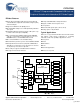
CY7C67300 Pin Diagram Figure 11.
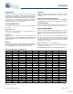
CY7C67300 Table 131.
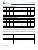
CY7C67300 Table 131.
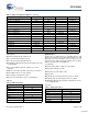
CY7C67300 Table 131.
CY7C67300 Absolute Maximum Ratings Max Output Current, per IO .......................................... 4 mA This section lists the absolute maximum ratings. Stresses above those listed can cause permanent damage to the device. Exposure to maximum rated conditions for extended periods can affect device operation and reliability. Operating Conditions Storage Temperature .................................. –40°C to +125°C TA (Ambient Temperature Under Bias) .........
CY7C67300 Table 133. DC Characteristics (continued)[8] Parameter ISLEEP Description Sleep Current Conditions Min USB Peripheral: includes 1.5K internal pull up Without 1.5K internal pull up ISLEEPB Sleep Current with Booster Enabled USB Peripheral: includes 1.5K internal pull up Without 1.5K internal pull up Typ. Max Unit 210 500 μA 5 30 μA 190 500 μA 5 30 μA Typ. Max Unit 5.25 V Table 134.
CY7C67300 AC Timing Characteristics Reset Timing tRESET nRESET tIOACT nRD or nWRL or nWRH Reset Timing Table 135. Reset Timing Parameters Parameter Description Min Typical Max Unit tRESET nRESET Pulse Width 16 clocks[11] tIOACT nRESET HIGH to nRD or nWRx active 200 µs Clock Timing tCLK tLOW XTALIN tFALL tHIGH tRISE Clock Timing Table 136. Clock Timing Parameters Parameter Description fCLK Clock Frequency vXINH[12] Clock Input High (XTALOUT left floating) Min Max 12.
CY7C67300 SRAM Read Cycle[15] Address CS t AR tCR t RPW RD t CDH t RDH t AC Din Data Valid Table 137. SRAM Read Cycle Parameters Parameter Description Min Typical Max Unit tCR CS LOW to RD LOW 1 ns tRDH RD HIGH to Data Hold 0 ns tCDH CS HIGH to Data Hold 0 ns tRPW[13] RD LOW Time 38 tAR tAC [14] 45 ns RD LOW to Address Valid 0 ns RAM Access to Data Valid 12 ns Notes 13. 0 wait state cycle. 14. tAC External SRAM access time = 12 ns for zero and one wait states.
CY7C67300 SRAM Write Cycle [17] Address t AW tCSW CS tWC t WPW WE t DW Dout t DH Data Valid Table 138. SRAM Write Cycle Parameters Parameter Description Min Typical Max Unit tAW Write Address Valid to WE LOW 7 ns tCSW CS LOW to WE LOW 7 ns tDW Data Valid to WE HIGH 15 ns tWPW[16] WE Pulse Width 15 ns tDH Data Hold from WE HIGH 4.5 ns tWC WE HIGH to CS HIGH 13 ns Notes 16. tWPW The write pulse width = 18.8 ns min. for zero and one wait states. The write pulse = 18.
CY7C67300 I2C EEPROM Timing-Serial IO tHIGH tLOW tR tF SCL tSU.STA tHD.STA tSU.DAT tHD.DAT tSU.STO tBUF SDA IN tAA tDH SDA OUT Table 139. I2C EEPROM Timing Parameters Parameter Description Min Typical Max Unit 400 kHz fSCL Clock Frequency tLOW Clock Pulse Width Low 1300 ns tHIGH Clock Pulse Width High 600 ns tAA Clock Low to Data Out Valid 900 ns tBUF Bus Idle Before New Transmission 1300 ns tHD.STA Start Hold Time 600 ns tSU.STA Start Setup Time 600 ns tHD.
CY7C67300 HPI (Host Port Interface) Write Cycle Timing tCYC tASU tWP tAH ADDR [1:0] tCSH tCSSU nCS nWR nRD Dout [15:0] tDSU tWDH Table 140. HPI Write Cycle Timing Parameters Parameter Description Min Typical Max Unit tASU Address Setup –1 ns tAH Address Hold –1 ns tCSSU Chip Select Setup –1 ns tCSH Chip Select Hold –1 ns tDSU Data Setup 6 ns tWDH Write Data Hold 2 ns tWP Write Pulse Width 2 T[18] tCYC Write Cycle Time 6 T[18] Notes 18.
CY7C67300 HPI (Host Port Interface) Read Cycle Timing tCYC tASU tRP tAH ADDR [1:0] tCSH tCSSU nCS tRDH nWR nRD Din [15:0] tACC tRDH Table 141.
CY7C67300 IDE Timing The IDE interface supports PIO mode 0-4 as specified in the Information Technology-AT Attachment–4 with Packet Interface Extension (ATA/ATAPI-4) Specification, T13/1153D Rev 18.
CY7C67300 Hardware CTS/RTS Handshake tCTShold tCTShold tCTSsetup tCTSsetup HSS_RTS HSS_CTS HSS_TxD Start of transmission not delayed by HSS_CTS Start of transmission delayed until HSS_CTS goes high tCTSsetup: HSS_CTS setup time before HSS_RTS = 1.5T min. tCTShold: HSS_CTS hold time after START bit = 0 ns min. T = 1/48 MHz. When RTS/CTS hardware handshake is enabled, transmission can be help off by deasserting HSS_CTS at least 1.5T before HSS_RTS. Transmission resumes when HSS_CTS returns HIGH.
CY7C67300 Table 142. Register Summary (continued) R/W R/W Address Register 0xC00C Watchdog Timer Bit 15 Bit 14 Bit 13 Bit 12 Bit 11 Bit 10 Bit 9 Bit 8 Default High Bit 7 Bit 6 Bit 5 Bit 4 Bit 3 Bit 2 Bit 1 Bit 0 Default Low Timeout Flag Period Select Lock Enable WDT Enable Reset Strobe 0000 0000 Reserved... 0000 0000 ...
CY7C67300 Table 142. Register Summary (continued) R/W R/W Address Register 0xC07E HSS Transmit Counter Bit 15 Bit 14 Bit 13 Bit 12 Bit 11 Bit 10 Bit 9 Bit 8 Default High Bit 7 Bit 6 Bit 5 Bit 4 Bit 3 Bit 2 Bit 1 Bit 0 Default Low Reserved Counter... 0000 0000 ...
CY7C67300 Table 142.
CY7C67300 Table 142. Register Summary (continued) R/W R/W R/W Address Register 0: PWM n Stop 0xC0EC 1: 0xC0F0 2: 0xC0F4 3: 0xC0F8 0xC0FA PWM Cycle Count Bit 15 Bit 14 Bit 13 Bit 12 Bit 11 Bit 10 Bit 9 Bit 8 Default High Bit 7 Bit 6 Bit 5 Bit 4 Bit 3 Bit 2 Bit 1 Bit 0 Default Low Reserved Address... 0000 0000 ...Address 0000 0000 Count... 0000 0000 ...Count R HPI Status Port VBUS Flag 0000 0000 ID Flag Reserved Resume2 Flag Resume1 Flag SIE2msg Document #: 38-08015 Rev.
CY7C67300 Ordering Information Table 143. Ordering Information Ordering Code Package Type AEC CY7C67300-100AXI 100 TQFP CY7C67300-100AXA 100 TQFP CY7C67300-100AXIT 100 TQFP, tape and reel CY7C67300-100AXAT 100 TQFP, tape and reel CY3663 Development Kit Pb-Free Temperature Range X –40 to 85°C X X X –40 to 85°C X –40 to 85°C X –40 to 85°C Package Diagrams Figure 12. 100-Pin Thin Plastic Quad Flat Pack (TQFP) A100SA NOTE: 16.00±0.25 SQ 1. JEDEC STD REF MS-026 14.00±0.05 SQ 100 2.
CY7C67300 Document History Page Document Title: CY7C67300 EZ-Host™ Programmable Embedded USB Host and Peripheral Controller with Automotive AEC Grade Support Document Number: 38-08015 REV. ECN NO. Orig.
CY7C67300 Sales, Solutions, and Legal Information Worldwide Sales and Design Support Cypress maintains a worldwide network of offices, solution centers, manufacturer’s representatives, and distributors. To find the office closest to you, visit us at cypress.com/sales. Products PSoC Clocks & Buffers PSoC Solutions psoc.cypress.com clocks.cypress.com General Low Power/Low Voltage psoc.cypress.com/solutions psoc.cypress.com/low-power Wireless wireless.cypress.com Precision Analog Memories memory.