CYS25G0101DX-ATC Evaluation Board User’s Guide Cypress Semiconductor Corporation • 3901 North First Street • San Jose • CA 95134 • 408-943-2600 March 19, 2002 [+] Feedback
CYS25G0101DX-ATC Evaluation Board User’s Guide Table of Contents 1. Introduction ....................................................................................................................................... 4 2. Features ............................................................................................................................................. 4 3. Kit Contents ........................................................................................................................
CYS25G0101DX-ATC Evaluation Board User’s Guide List of Figures (continued) Figure 23. Reference Clock Block Schematic Diagram ................................................................... 31 Figure 24. CYS25G0101DX Evaluation Board PCB Mechanical Drawing ....................................... 33 Figure 25. CYS25G0101DX Evaluation Board PCB Top Layer Silk Screen .................................... 34 Figure 26. CYS25G0101DX Evaluation Board PCB Top Layer Layout ......................................
CYS25G0101DX-ATC Evaluation Board User’s Guide 1. Introduction Cypress's CYS25G0101DX SONET OC-48 Transceiver is a communications building block for high-speed SONET data communications. It provides complete parallel-to-serial and serial-to-parallel conversions, clock generation, and clock and data recovery operations in a single chip, optimized for full SONET/SDH compliance.
CYS25G0101DX-ATC Evaluation Board User’s Guide (155.52MHz) FIFO_RST TXCLKI FIFO_ERR TXD 15:0 (155.52MHz) REFCLK TXCLKO (155.52MHz) RXCLKOUT RXD 15:0 Output Register Input Register TX PLL x16 FIFO (5byte) SHIFTER Recovered Bit-Clock /16 SHIFTER /16 RX CDR PLL Tx Bit-Clock Lock-to-Ref LOOPTIME Retimed Data DIAGLOOP LINELOOP LOOPA Lock-to-Data / Clock Control Logic OUT± PWRDN LOCKREF SD LFI RESET IN± Figure 1.
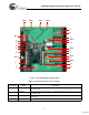
CYS25G0101DX-ATC Evaluation Board User’s Guide SMA13 SMA14 SMA16 SMA15 J4 P4 SW1 J5 SMA17 J6 P2 J7 D2 SMA18 D1 P3 J8 J3 SMA12 SMA11 P5 SMA10 J1 J2 P5 P1 Figure 2. The CYS25G0101DX Evaluation Board Table 1. Functional Description of the Connectors Jumpers and Connectors Name Description J1 RxD BUS 16-bit RxD Data Bus interface header (see Table 2 for details). Figure 3 shows the orientation of this header J2 TxD BUS 16-bit TxD Data Bus interface header (see Table 3 for details).
CYS25G0101DX-ATC Evaluation Board User’s Guide Table 1. Functional Description of the Connectors (continued) Jumpers and Connectors Name Description J5 SD This jumper is used to set the SD signal. When open (default), SD signal will be driven by the optical module. When 1-2 are shorted, SD is forced to HIGH. When 2-3 are shorted, SD is forced to LOW. Figure 3 shows the orientation of this jumper J6 TEST0 This jumper, when shorted, is to enable the Parallel Line Loopback mode.
CYS25G0101DX-ATC Evaluation Board User’s Guide Table 2. Pin Assignment of J1 Header and Description of J10 Header (continued) Pin Number Name I/O Characteristics Description 5 RXD13 HSTL output Parallel receive data output RXD13. The outputs change following RXCLK↓ 7 RXD12 HSTL output Parallel receive data output RXD12. The outputs change following RXCLK↓ 9 RXD11 HSTL output Parallel receive data output RXD11.
CYS25G0101DX-ATC Evaluation Board User’s Guide Table 3. Pin Assignment of J2 Header and Description of J9 Header (continued) Pin Number Name I/O Characteristics Description 8 TXD12 HSTL input Parallel transmit data input TXD12. The input data is sampled by TXCLKI↑ 10 TXD11 HSTL input Parallel transmit data input TXD10. The input data is sampled by TXCLKI↑ 12 TXD10 HSTL input Parallel transmit data input TXD9.
CYS25G0101DX-ATC Evaluation Board User’s Guide Table 4. Functional Description of DIP Switch 1 (SW1) (continued) Position Name State 5 LOOPTIME ON 6 LOCKREF 7 PWRDN 8 FIFO_RST Description The transmission will be using the extracted receive bit-clock for the transmitted bit clock OFF* The transmission will be using the REFCLK input (155.
CYS25G0101DX-ATC Evaluation Board User’s Guide 5A 1A 1B 5B J5 3 2 1 J7 LFI GND FIFO_ERR GND J8 TXCLKO GND J2 TXCLKI GND RXCLK GND J1 Pin 1 Pin 1 Figure 3.
CYS25G0101DX-ATC Evaluation Board User’s Guide 5. Diagnostic Modes The CYS25G0101DX Evaluation Board provides four different diagnostic modes—Diagnostic Loopback mode, Line Loopback mode, Analog Loopback mode and “Parallel Line Loopback” mode. Figure 4 to Figure 7 illustrate these diagnostic modes and Figure 8 to Figure 10 illustrate the testing equipment set-up for testing the characteristics of the CYS25G0101DX. 5.
CYS25G0101DX-ATC Evaluation Board User’s Guide 5.2 Line Loopback In the Line Loopback mode, serial data (from IN±) will loop through the serial input buffer and CDR block to the serial output buffer (OUT±). Figure 5 shows the data path (bold line) of the Line Loopback mode. To select the Line Loopback mode: 1. SW1-3 (LINELOOP) must be in ON position 2. All other dip switch settings must be in their default positions as stated in Table 4 3. TEST0, jumper J6 must be opened 4.
CYS25G0101DX-ATC Evaluation Board User’s Guide 5.3 Analog Line Loopback In the Analog Line Loopback mode, serial data (from IN±) will loop through directly from serial input buffer to the serial output buffer (OUT±). Figure 6 shows the data path (bold line) of the Analog Line Loopback mode. To select the Analog Line Loopback mode: 1. SW1-4 (LOOPA) must be in ON position and SW1-3 (LINELOOP) must be in OFF position. 2. All other dip switches must be in their default positions as stated in Table 4 3.
CYS25G0101DX-ATC Evaluation Board User’s Guide 5.4 “Parallel Line Loopback” (TEST0) Mode In Parallel Line Loopback mode, the parallel output buffers are internally linked to the parallel input buffers. Figure 7 shows the data path (bold line) of the Parallel Line Loopback mode. In this test mode, the internal RX CDR PLL and TX PLL can be tested by different configurations. 5.4.1 Test the Internal RX CDR PLL Only 1. TEST0, jumper J6 must be shorted 2. SW1-5 (LOOPTIME) must be in ON position 3.
CYS25G0101DX-ATC Evaluation Board User’s Guide 6. Testing Hookup 6.1 Set-up for BERT Test Figure 8 illustrates the set-up for the BERT test. The equipment list: 1. Evaluation Board – Cypress CYS25G0101DX Evaluation Board 2. Pattern Generator – Tektronix D3186 Pattern Generator 3. Error Detector– Tektronix D3286 Error Detector 4.
CYS25G0101DX-ATC Evaluation Board User’s Guide 6.2 Set-up for Eye Diagram Test Figure 9 illustrates the set-up for testing the Eye Diagram. The equipment list : 1. Evaluation Board – Cypress CYS25G0101DX Evaluation Board 2. Pattern Generator – Tektronix D3186 Pattern Generator 3. Oscilloscope – Agilent Infiniium DCA 86100A with 83484A Dual-Channel 50GHz Module 4.
CYS25G0101DX-ATC Evaluation Board User’s Guide 6.3 SONET Jitter Transfer and Jitter Tolerance Test Figure 10 illustrates the set-up for testing the jitter. The equipment list: 1. Evaluation Board – Cypress CYS25G0101DX Evaluation Board 2. SONET Tester – Agilent (HP) OmniBER 718 Communication Performance Analyzer 3. Optical Converters - Agilent (HP) 83446A Receiver and 83430A Transmitter 4.
CYS25G0101DX-ATC Evaluation Board User’s Guide 6.4 Set-up for Testing the TX PLL in Parallel Line Loopback Mode Figure 11 illustrates the set-up for testing the TX PLL in Parallel Line Loopback Mode. The equipment list : 1. Evaluation Board – Cypress CYS25G0101DX Evaluation Board 2. Pattern Generator – Tektronix D3186 Pattern Generator 3. Error Detector– Tektronix D3286 Error Detector 4. Pulse Generator - HP 8133A Pulse Generator 5.
CYS25G0101DX-ATC Evaluation Board User’s Guide 7. Eye Diagram Testing Result Figure 12 is the Eye Diagram measurement from CYS25G0101DX Evaluation Board by using the test set-up as in Figure 9. In this measurement, the evaluation board is configured to parallel loop back mode (Figure 7) and with no SONET filter at the oscilloscope. Figure 12.
CYS25G0101DX-ATC Evaluation Board User’s Guide 8. Jitter Transfer Testing Result Figure 13 and Figure 14 show the Jitter Transfer measurement by using the test set-up as in Figure 10. Figure 13 is the measurement result of the GR-253 (Bellcore) standard and Figure 14 is the measurement result of the G958 (ITU) standard. In this measurement, the CYS25G0101DX evaluation board is configured to parallel loopback mode (Figure 7). Figure 13.
CYS25G0101DX-ATC Evaluation Board User’s Guide 9. Jitter Tolerance Testing Result Figure 15 and Figure 16 show the Jitter Tolerance measurement by using the test set-up as in Figure 10. Figure 15 is the measurement result of the GR-253 (Bellcore) standard and Figure 16 is the measurement result of the G825 (ITU) standard. In this measurement, the CYS25G0101DX evaluation board is configured to parallel loopback mode (Figure 7). Figure 15.
CYS25G0101DX-ATC Evaluation Board User’s Guide 10. Schematic Diagram, PCB Layout and BOM (Bill of Material) Figure 17 to Figure 23 in Appendix A shows the schematic diagram of the CYS25G0101DX evaluation board. Figure 17 is the top level diagram for the schematic diagrams for Figure 18 to Figure 23. Figure 24 to Figure 32 in Appendix B show the PCB layout of each layer of the CYS25G0101DX evaluation board.
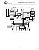
CYS25G0101DX-ATC Evaluation Board User’s Guide Appendix A: Schematic Diagrams of the CYS25G0101DX Evaluation Board 24 [+] Feedback
Control Block Parallel Input Block Reference Clock Block Parallel Output Block Power Supply Block Signals Block o CYS25G0101DX-ATC Evaluation Board User’s Guide Figure 17.
CYS25G0101DX-ATC Evaluation Board User’s Guide Figure 18.
CYS25G0101DX-ATC Evaluation Board User’s Guide Figure 19.
CYS25G0101DX-ATC Evaluation Board User’s Guide Figure 20.
CYS25G0101DX-ATC Evaluation Board User’s Guide Figure 21.
CYS25G0101DX-ATC Evaluation Board User’s Guide Figure 22.
CYS25G0101DX-ATC Evaluation Board User’s Guide Figure 23.
CYS25G0101DX-ATC Evaluation Board User’s Guide Appendix B: PCB Layout Diagrams of the CYS25G0101DX Evaluation Board 32 [+] Feedback
CYS25G0101DX-ATC Evaluation Board User’s Guide Figure 24.
CYS25G0101DX-ATC Evaluation Board User’s Guide Figure 25.
CYS25G0101DX-ATC Evaluation Board User’s Guide Figure 26.
CYS25G0101DX-ATC Evaluation Board User’s Guide Figure 27.
CYS25G0101DX-ATC Evaluation Board User’s Guide Figure 28.
CYS25G0101DX-ATC Evaluation Board User’s Guide Figure 29.
CYS25G0101DX-ATC Evaluation Board User’s Guide Figure 30.
CYS25G0101DX-ATC Evaluation Board User’s Guide Figure 31.
CYS25G0101DX-ATC Evaluation Board User’s Guide Figure 32.
CYS25G0101DX-ATC Evaluation Board User’s Guide Appendix C: CYS25G0101DX Evaluation Board LVPECL BOM (Bill of Material) 42 [+] Feedback
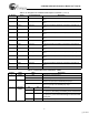
CYS25G0101DX-ATC Evaluation Board User’s Guide Table 8.
CYS25G0101DX-ATC Evaluation Board User’s Guide Table 9.
CYS25G0101DX-ATC Evaluation Board User’s Guide Table 10.
CYS25G0101DX-ATC Evaluation Board User’s Guide Table 11.
CYS25G0101DX-ATC Evaluation Board User’s Guide Appendix D: CYS25G0101DX Evaluation Board HSTL BOM (Bill of Material) 47 [+] Feedback
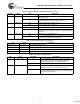
CYS25G0101DX-ATC Evaluation Board User’s Guide Table 12.
CYS25G0101DX-ATC Evaluation Board User’s Guide Table 13.
CYS25G0101DX-ATC Evaluation Board User’s Guide Table 14.
CYS25G0101DX-ATC Evaluation Board User’s Guide Table 15. CYS25G0101DX Evaluation Board HSTL BOM - Page 4 of 4 © Cypress Semiconductor Corporation, 2002. The information contained herein is subject to change without notice. Cypress Semiconductor Corporation assumes no responsibility for the use of any circuitry other than circuitry embodied in a Cypress Semiconductor product. Nor does it convey or imply any license under patent or other rights.