CY8C24123A CY8C24223A, CY8C24423A PSoC® Programmable System-on-Chip™ Features ■ ■ ■ ■ ■ Powerful Harvard Architecture Processor ❐ M8C Processor Speeds to 24 MHz ❐ 8x8 Multiply, 32-Bit Accumulate ❐ Low Power at High Speed ❐ 2.4 to 5.25V Operating Voltage ❐ Operating Voltages Down to 1.
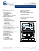
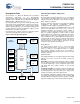
CY8C24123A CY8C24223A, CY8C24423A The PSoC family consists of many Mixed-Signal Array with On-Chip Controller devices. These devices are designed to replace multiple traditional MCU-based system components with a low cost single-chip programmable device. PSoC devices include configurable blocks of analog and digital logic, and programmable interconnects. This architecture enables the user to create customized peripheral configurations that match the requirements of each individual application.
CY8C24123A CY8C24223A, CY8C24423A The Analog System consists of six configurable blocks, each consisting of an opamp circuit that allows the creation of complex analog signal flows. Analog peripherals are very flexible and can be customized to support specific application requirements. Some of the more common PSoC analog functions (most available as user modules) are: ■ ■ Analog-to-digital converters (up to two, with 6 to 14-bit resolution, selectable as Incremental, Delta Sigma, and SAR) Figure 2.
CY8C24123A CY8C24223A, CY8C24423A Getting Started Additional System Resources System Resources, some of which are listed in the previous sections, provide additional capability useful to complete systems. Additional resources include a multiplier, decimator, switch mode pump, low voltage detection, and power on reset. Statements describing the merits of each system resource follow: ■ Digital clock dividers provide three customizable clock frequencies for use in applications.
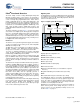
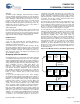
CY8C24123A CY8C24223A, CY8C24423A Development Tools PSoC Designer Software Subsystems PSoC Designer is a Microsoft® Windows-based, integrated development environment for the Programmable System-on-Chip (PSoC) devices. The PSoC Designer IDE and application runs on Windows NT 4.0, Windows 2000, Windows Millennium (Me), or Windows XP (refer Figure 3).
CY8C24123A CY8C24223A, CY8C24423A Debugger The PSoC Designer Debugger subsystem provides hardware in-circuit emulation, allowing the designer to test the program in a physical system while providing an internal view of the PSoC device. Debugger commands allow the designer to read and program and read and write data memory, read and write IO registers, read and write CPU registers, set and clear breakpoints, and provide program run, halt, and step control.
CY8C24123A CY8C24223A, CY8C24423A The next step is to write your main program, and any sub-routine using PSoC Designer’s Application Editor subsystem. The Application Editor includes a Project Manager that allows you to open the project source code files (including all generated code files) from a hierarchal view. The source code editor provides syntax coloring and advanced edit features for both C and assembly language.
CY8C24123A CY8C24223A, CY8C24423A Pinouts This section describes, lists, and illustrates the CY8C24x23A PSoC device pins and pinout configurations. Every port pin (labeled with a “P”) is capable of Digital IO. However, Vss, Vdd, SMP, and XRES are not capable of Digital IO. 8-Pin Part Pinoutt Table 3. Pin Definitions - 8-Pin PDIP and SOIC Pin No.
CY8C24123A CY8C24223A, CY8C24423A 20-Pin Part Pinout Table 4. Pin Definitions - 20-Pin PDIP, SSOP, and SOIC Pin No.
CY8C24123A CY8C24223A, CY8C24423A 28-Pin Part Pinout Table 5. Pin Definitions - 28-Pin PDIP, SSOP, and SOIC Pin No.
CY8C24123A CY8C24223A, CY8C24423A 32-Pin Part Pinout Table 6.
CY8C24123A CY8C24223A, CY8C24423A 56-Pin Part Pinout The 56-pin SSOP part is for the CY8C24000A On-Chip Debug (OCD) PSoC device. Note This part is only used for in-circuit debugging. It is NOT available for production. Table 7. Pin Definitions - 56-Pin SSOP Pin No.
CY8C24123A CY8C24223A, CY8C24423A Table 7. Pin Definitions - 56-Pin SSOP (continued) 34 35 36 37 38 39 40 41 Type Digital Analog IO IO IO IO IO IO IO Input 42 43 44 45 46 47 48 OCD OCD IO IO IO IO IO I 49 IO I 50 51 IO IO 52 53 IO IO I I 54 IO I 55 56 IO Power I Pin No. Pin Name Description P1[6] P5[0] P5[2] P3[0] P3[2] P3[4] P3[6] XRES Active high external reset with internal pull down. HCLK OCD high-speed clock output. CCLK OCD CPU clock output.
CY8C24123A CY8C24223A, CY8C24423A Register Reference Register Mapping Tables This section lists the registers of the CY8C24x23A PSoC device. For detailed register information, refer the PSoC Programmable Sytem-on-Chip Reference Manual. The PSoC device has a total register address space of 512 bytes. The register space is referred to as IO space and is divided into two banks. The XOI bit in the Flag register (CPU_F) determines which bank the user is currently in.
CY8C24123A CY8C24223A, CY8C24423A Table 9.
CY8C24123A CY8C24223A, CY8C24423A Table 9. Register Map Bank 0 Table: User Space (continued) Addr Access Name (0,Hex) 3E 3F Blank fields are Reserved and must not be accessed. Name Addr (0,Hex) 7E 7F Access Addr (0,Hex) BE BF # Access is bit specific. Name Access Name CPU_SCR1 CPU_SCR0 Addr (0,Hex) FE FF Access # # Table 10.
CY8C24123A CY8C24223A, CY8C24423A Table 10. Register Map Bank 1 Table: Configuration Space (continued) Addr Access Name (1,Hex) 37 ACB01CR2 38 39 3A 3B 3C 3D 3E 3F Blank fields are Reserved and must not be accessed. Name Document Number: 38-12028 Rev. *I Addr (1,Hex) 77 78 79 7A 7B 7C 7D 7E 7F Access RW Addr (1,Hex) B7 B8 B9 BA BB BC BD BE BF # Access is bit specific.
CY8C24123A CY8C24223A, CY8C24423A Electrical Specifications This section presents the DC and AC electrical specifications of the CY8C24x23A PSoC device. For the latest electrical specifications, check if you have the most recent data sheet by visiting the web at http://www.cypress.com/psoc. Specifications are valid for -40°C ≤ TA ≤ 85°C and TJ ≤ 100°C, except where noted. Refer to Table 31 on page 32 for the electrical specifications on the internal main oscillator (IMO) using SLIMO mode. Figure 11.
CY8C24123A CY8C24223A, CY8C24423A Absolute Maximum Ratings Exceeding maximum ratings may shorten the useful life of the device. User guidelines are not tested. Table 12. Absolute Maximum Ratings Symbol Description TSTG Storage Temperature Min -55 Typ 25 Max +100 TA Vdd VIO Ambient Temperature with Power Applied Supply Voltage on Vdd Relative to Vss DC Input Voltage -40 -0.5 Vss - 0.5 – – – VIOZ DC Voltage Applied to Tri-state Vss - 0.
CY8C24123A CY8C24223A, CY8C24423A DC Electrical Characteristics DC Chip-Level Specifications Table 14 lists the guaranteed maximum and minimum specifications for the voltage and temperature ranges: 4.75V to 5.25V and -40°C ≤ TA ≤ 85°C, 3.0V to 3.6V and -40°C ≤ TA ≤ 85°C, or 2.4V to 3.0V and -40°C ≤ TA ≤ 85°C, respectively. Typical parameters apply to 5V, 3.3V, and 2.7V at 25°C and are for design guidance only. Table 14. DC Chip-Level Specifications Symbol Description Vdd Supply Voltage Min 2.
CY8C24123A CY8C24223A, CY8C24423A DC General Purpose IO Specifications The following tables list the guaranteed maximum and minimum specifications for the voltage and temperature ranges: 4.75V to 5.25V and -40°C ≤ TA ≤ 85°C, 3.0V to 3.6V and -40°C ≤ TA ≤ 85°C, or 2.4V to 3.0V and -40°C ≤ TA ≤ 85°C, respectively. Typical parameters apply to 5V, 3.3V, and 2.7V at 25°C and are for design guidance only. Table 15. 5V and 3.
CY8C24123A CY8C24223A, CY8C24423A DC Operational Amplifier Specifications The following tables list the guaranteed maximum and minimum specifications for the voltage and temperature ranges: 4.75V to 5.25V and -40°C ≤ TA ≤ 85°C, 3.0V to 3.6V and -40°C ≤ TA ≤ 85°C, or 2.4V to 3.0V and -40°C ≤ TA ≤ 85°C, respectively. Typical parameters apply to 5V, 3.3V, and 2.7V at 25°C and are for design guidance only.
CY8C24123A CY8C24223A, CY8C24423A Table 18. 3.3V DC Operational Amplifier Specifications Symbol VOSOA Description Input Offset Voltage (absolute value) Power = Low, Opamp Bias = High Power = Medium, Opamp Bias = High High Power is 5 Volts Only TCVOSOA Average Input Offset Voltage Drift Min Typ Max Units – – 1.65 1.32 10 8 mV mV – 7.0 35.0 μV/°C Notes IEBOA Input Leakage Current (Port 0 Analog Pins) – 20 – pA Gross tested to 1 μA CINOA Input Capacitance (Port 0 Analog Pins) – 4.
CY8C24123A CY8C24223A, CY8C24423A Table 19. 2.7V DC Operational Amplifier Specifications Symbol VOSOA Description Input Offset Voltage (absolute value) Power = Low, Opamp Bias = High Power = Medium, Opamp Bias = High High Power is 5 Volts Only TCVOSOA Average Input Offset Voltage Drift Min Typ Max Units – – 1.65 1.32 10 8 mV mV – 7.0 35.0 μV/°C Notes IEBOA Input Leakage Current (Port 0 Analog Pins) – 20 – pA Gross tested to 1 μA CINOA Input Capacitance (Port 0 Analog Pins) – 4.
CY8C24123A CY8C24223A, CY8C24423A DC Analog Output Buffer Specifications The following tables list the guaranteed maximum and minimum specifications for the voltage and temperature ranges: 4.75V to 5.25V and -40°C ≤ TA ≤ 85°C, 3.0V to 3.6V and -40°C ≤ TA ≤ 85°C, or 2.4V to 3.0V and -40°C ≤ TA ≤ 85°C, respectively. Typical parameters apply to 5V, 3.3V, and 2.7V at 25°C and are for design guidance only. Table 21.
CY8C24123A CY8C24223A, CY8C24423A Table 23. 2.7V DC Analog Output Buffer Specifications Symbol Typ Max – 3 12 mV – +6 – μV/°C 0.5 - Vdd - 1.0 V – – 1 1 – – W W VOHIGHOB High Output Voltage Swing (Load = 1k ohms to Vdd/2) Power = Low 0.5 x Vdd + 0.2 Power = High 0.5 x Vdd + 0.2 – – – – VOLOWOB Low Output Voltage Swing (Load = 1k ohms to Vdd/2) Power = Low Power = High – – – – 0.5 x Vdd - 0.7 0.5 x Vdd - 0.
CY8C24123A CY8C24223A, CY8C24423A Table 24. DC Switch Mode Pump (SMP) Specifications (continued) Symbol Description Min Typ Max Units Notes ΔVPUMP_Line Line Regulation (over VBAT range) – 5 – %VO Configuration listed in footnote.a VO is the “Vdd Value for PUMP Trip” specified by the VM[2:0] setting in the DC POR and LVD Specification, Table 29 on page 30. ΔVPUMP_Load Load Regulation – 5 – %VO Configuration listed in footnote.
CY8C24123A CY8C24223A, CY8C24423A DC Analog Reference Specifications The following tables list the guaranteed maximum and minimum specifications for the voltage and temperature ranges: 4.75V to 5.25V and -40°C ≤ TA ≤ 85°C, 3.0V to 3.6V and -40°C ≤ TA ≤ 85°C, or 2.4V to 3.0V and -40°C ≤ TA ≤ 85°C, respectively. Typical parameters apply to 5V, 3.3V, and 2.7V at 25°C and are for design guidance only. The guaranteed specifications are measured through the Analog Continuous Time PSoC blocks.
CY8C24123A CY8C24223A, CY8C24423A Table 26. 3.3V DC Analog Reference Specifications (continued) Symbol Description Min Typ Max Units – RefHi = P2[4] + P2[6] (P2[4] = Vdd/2, P2[4] + P2[6] - 0.075 P2[4] + P2[6] - 0.009 P2[4] + P2[6] + 0.057 V P2[6] = 0.5V) – RefHi = 3.2 x BandGap Not Allowed – RefLo = Vdd/2 - BandGap Not Allowed – RefLo = BandGap Not Allowed – RefLo = 2 x BandGap - P2[6] (P2[6] = 0.
CY8C24123A CY8C24223A, CY8C24423A DC Analog PSoC Block Specifications Table 29 lists the guaranteed maximum and minimum specifications for the voltage and temperature ranges: 4.75V to 5.25V and -40°C ≤ TA ≤ 85°C, 3.0V to 3.6V and -40°C ≤ TA ≤ 85°C, or 2.4V to 3.0V and -40°C ≤ TA ≤ 85°C, respectively. Typical parameters apply to 5V, 3.3V, and 2.7V at 25°C and are for design guidance only. Table 28.
CY8C24123A CY8C24223A, CY8C24423A DC Programming Specifications Table 31 lists the guaranteed maximum and minimum specifications for the voltage and temperature ranges: 4.75V to 5.25V and -40°C ≤ TA ≤ 85°C, 3.0V to 3.6V and -40°C ≤ TA ≤ 85°C, or 2.4V to 3.0V and -40°C ≤ TA ≤ 85°C, respectively. Typical parameters apply to 5V, 3.3V, and 2.7V at 25°C and are for design guidance only. Table 30. DC Programming Specifications Symbol Description VddIWRIT Supply Voltage for Flash Write Operations Min 2.
CY8C24123A CY8C24223A, CY8C24423A AC Electrical Characteristics AC Chip-Level Specifications The following tables list the guaranteed maximum and minimum specifications for the voltage and temperature ranges: 4.75V to 5.25V and -40°C ≤ TA ≤ 85°C, 3.0V to 3.6V and -40°C ≤ TA ≤ 85°C, or 2.4V to 3.0V and -40°C ≤ TA ≤ 85°C, respectively. Typical parameters apply to 5V, 3.3V, and 2.7V at 25°C and are for design guidance only. Table 31. 5V and 3.
CY8C24123A CY8C24223A, CY8C24423A Table 32. 2.7V AC Chip-Level Specifications Symbol FIMO12 Description Internal Main Oscillator Frequency for 12 MHz Min 11.5 Typ 12 FIMO6 Internal Main Oscillator Frequency for 6 MHz 5.75 6 FCPU1 FBLK27 CPU Frequency (2.7V Nominal)0 Digital PSoC Block Frequency (2.
CY8C24123A CY8C24223A, CY8C24423A Figure 14. PLL Lock Timing Diagram PLL Enable TPLLSLEW 24 MHz FPLL PLL Gain 0 Figure 15. PLL Lock for Low Gain Setting Timing Diagram PLL Enable TPLLSLEWLOW 24 MHz FPLL PLL Gain 1 Figure 16. External Crystal Oscillator Startup Timing Diagram 32K Select 32 kHz TOS F32K2 Figure 17. 24 MHz Period Jitter (IMO) Timing Diagram Jitter24M1 F 24M Figure 18. 32 kHz Period Jitter (ECO) Timing Diagram Jitter32k F 32K2 Document Number: 38-12028 Rev.
CY8C24123A CY8C24223A, CY8C24423A AC General Purpose IO Specifications The following tables list the guaranteed maximum and minimum specifications for the voltage and temperature ranges: 4.75V to 5.25V and -40°C ≤ TA ≤ 85°C, 3.0V to 3.6V and -40°C ≤ TA ≤ 85°C, or 2.4V to 3.0V and -40°C ≤ TA ≤ 85°C, respectively. Typical parameters apply to 5V, 3.3V, and 2.7V at 25°C and are for design guidance only. Table 33. 5V and 3.
CY8C24123A CY8C24223A, CY8C24423A AC Operational Amplifier Specifications The following tables list the guaranteed maximum and minimum specifications for the voltage and temperature ranges: 4.75V to 5.25V and -40°C ≤ TA ≤ 85°C, 3.0V to 3.6V and -40°C ≤ TA ≤ 85°C, or 2.4V to 3.0V and -40°C ≤ TA ≤ 85°C, respectively. Typical parameters apply to 5V, 3.3V, and 2.7V at 25°C and are for design guidance only. Settling times, slew rates, and gain bandwidth are based on the Analog Continuous Time PSoC block.
CY8C24123A CY8C24223A, CY8C24423A Table 37. 2.7V AC Operational Amplifier Specifications Symbol TROA TSOA Min Typ Max Units Rising Settling Time from 80% of ΔV to 0.1% of ΔV (10 pF load, Unity Gain) Power = Low, Opamp Bias = Low Power = Medium, Opamp Bias = High Description – – – – 3.92 0.72 μs μs Falling Settling Time from 20% of ΔV to 0.1% of ΔV (10 pF load, Unity Gain) Power = Low, Opamp Bias = Low Power = Medium, Opamp Bias = High – – – – 5.41 0.
CY8C24123A CY8C24223A, CY8C24423A When bypassed by a capacitor on P2[4], the noise of the analog ground signal distributed to each block is reduced by a factor of up to 5 (14 dB). This is at frequencies above the corner frequency defined by the on-chip 8.1k resistance and the external capacitor. Figure 20. Typical AGND Noise with P2[4] Bypass dBV/rtHz 10000 0 0.01 0.1 1.0 10 1000 100 0.001 0.01 0.
CY8C24123A CY8C24223A, CY8C24423A AC Low Power Comparator Specifications Table 38 lists the guaranteed maximum and minimum specifications for the voltage and temperature ranges: 4.75V to 5.25V and -40°C ≤ TA ≤ 85°C, 3.0V to 3.6V and -40°C ≤ TA ≤ 85°C, or 2.4V to 3.0V and -40°C ≤ TA ≤ 85°C, respectively. Typical parameters apply to 5V at 25°C and are for design guidance only. Table 38.
CY8C24123A CY8C24223A, CY8C24423A Table 40. 2.7V AC Digital Block Specifications Function Description Min Typ Max Units 12.7 MHz –0 –0 ns All Maximum Block Clocking Frequency Functions Timer Capture Pulse Width Maximum Frequency, With or Without Capture Counter Dead Band 100a – – 12.7 MHz 100a –0 –0 ns Maximum Frequency, No Enable Input – – 12.7 MHz Maximum Frequency, Enable Input – – 12.
CY8C24123A CY8C24223A, CY8C24423A AC Analog Output Buffer Specifications The following tables list the guaranteed maximum and minimum specifications for the voltage and temperature ranges: 4.75V to 5.25V and -40°C ≤ TA ≤ 85°C, 3.0V to 3.6V and -40°C ≤ TA ≤ 85°C, or 2.4V to 3.0V and -40°C ≤ TA ≤ 85°C, respectively. Typical parameters apply to 5V, 3.3V, and 2.7V at 25°C and are for design guidance only. Table 41.
CY8C24123A CY8C24223A, CY8C24423A Table 43. 2.7V AC Analog Output Buffer Specifications Symbol Description Min Typ Max Units TROB Rising Settling Time to 0.1%, 1V Step, 100 pF Load Power = Low Power = High – – – – 4 4 μs μs TSOB Falling Settling Time to 0.1%, 1V Step, 100 pF Load Power = Low Power = High – – – – 3 3 μs μs SRROB Rising Slew Rate (20% to 80%), 1V Step, 100 pF Load Power = Low Power = High 0.4 0.
CY8C24123A CY8C24223A, CY8C24423A Table 46. 2.7V AC External Clock Specifications Symbol Description FOSCEXT Frequency with CPU Clock divide by 1a FOSCEXT Frequency with CPU Clock divide by 2 or greaterb Min Typ Max Units 0.093 – 12.3 MHz 0.186 – 12.3 MHz – High Period with CPU Clock divide by 1 41.7 – 5300 ns – Low Period with CPU Clock divide by 1 41.7 – – ns – Power Up IMO to Switch 150 – – μs a. Maximum CPU frequency is 12 MHz at 3.3V.
CY8C24123A CY8C24223A, CY8C24423A Table 48. AC Characteristics of the I2C SDA and SCL Pins for Vdd > 3.0V (continued) Symbol Standard Mode Description Fast Mode Min Max Min Max Units TSUSTOI2C Setup Time for STOP Condition 4.0 – 0.6 – μs TBUFI2C Bus Free Time Between a STOP and START Condition 4.7 – 1.3 – μs TSPI2C Pulse Width of spikes are suppressed by the input filter. – – 0 50 ns a.
CY8C24123A CY8C24223A, CY8C24423A Packaging Information This section illustrates the packaging specifications for the CY8C24x23A PSoC device, along with the thermal impedances for each package and the typical package capacitance on crystal pins. Important Note Emulation tools may require a larger area on the target PCB than the chip’s footprint. For a detailed description of the emulation tools’ dimensions, refer to the document titled PSoC Emulator Pod Dimensions at http://www.cypress.com/design/MR10161.
CY8C24123A CY8C24223A, CY8C24423A Figure 24. 8-Pin (150-Mil) SOIC PIN 1 ID 1 4 1. DIMENSIONS IN INCHES[MM] MIN. MAX. 2. PIN 1 ID IS OPTIONAL, ROUND ON SINGLE LEADFRAME RECTANGULAR ON MATRIX LEADFRAME 0.150[3.810] 0.157[3.987] 3. REFERENCE JEDEC MS-012 0.230[5.842] 0.244[6.197] 4. PACKAGE WEIGHT 0.07gms PART # S08.15 STANDARD PKG. 5 SZ08.15 LEAD FREE PKG. 8 0.189[4.800] 0.196[4.978] 0.010[0.254] X 45° 0.016[0.406] SEATING PLANE 0.061[1.549] 0.068[1.727] 0.004[0.102] 0.050[1.270] BSC 0.
CY8C24123A CY8C24223A, CY8C24423A Figure 26. 20-Pin (210-Mil) SSOP 51-85077 *C Figure 27. 20-Pin (300-Mil) Molded SOIC 51-85024 *C Document Number: 38-12028 Rev.
CY8C24123A CY8C24223A, CY8C24423A Figure 28. 28-Pin (300-Mil) Molded DIP 51-85014 *D Figure 29. 28-Pin (210-Mil) SSOP 51-85079 *C Document Number: 38-12028 Rev.
CY8C24123A CY8C24223A, CY8C24423A Figure 30. 28-Pin (300-Mil) Molded SOIC 51-85026 *D Figure 31. 32-Pin (5x5 mm) QFN CHANGED SPEC. TITLE, CORRECTED EPAD DIMENSION TOP VIEW 01/29/07 JSO X = 138 MIL Y = 138 MIL SIDE VIEW BOTTOM VIEW32 3.50 PIN1 ID 0.20 R. Ø N N 1 2 1 2 0.45 SOLDERABLE EXPOSED 3.50 3.50 PAD -0.20 0°-12° AD X, Y for this product is 3.53 mm, 3.53 mm (+/-0.11 mm) 0.50 SEATING PLANE C 0.42±0.18 [4X] 3.50 NOTES: 1. HATCH AREA IS SOLDERABLE EXPOSED PAD. 2.
CY8C24123A CY8C24223A, CY8C24423A Figure 32. 32-Pin Sawn QFN Package SO LDERABLE EXPOSED PAD NOTES: 1. H A T C H A R E A IS S O LD E R A B LE E X P O S E D P A D 2 . B A S E D O N R E F J E D E C # M O -220 3 . P A C K A G E W E IG H T: 0.058g 001-30999 *A CYPRESS C O M P A N Y C O N F ID E N T IA L 4 .
CY8C24123A CY8C24223A, CY8C24423A Thermal Impedances Capacitance on Crystal Pins Table 50. Thermal Impedances per Package Table 51. Typical Package Capacitance on Crystal Pins Typical θJA * Package Package Package Capacitance 8 PDIP 123°C/W 8 PDIP 2.8 pF 8 SOIC 185°C/W 8 SOIC 2.0 pF 20 PDIP 109°C/W 20 PDIP 3.0 pF 20 SSOP 117 °C/W 20 SSOP 2.6 pF 20 SOIC 81°C/W 20 SOIC 2.5 pF 28 PDIP 69 °C/W 28 PDIP 3.5 pF 28 SSOP 101°C/W 28 SSOP 2.8 pF 28 SOIC 74 °C/W 28 SOIC 2.
CY8C24123A CY8C24223A, CY8C24423A Development Tool Selection ■ 110 ~ 240V Power Supply, Euro-Plug Adapter ■ iMAGEcraft C Compiler (Registration Required) ■ ISSP Cable Software ■ USB 2.0 Cable and Blue Cat-5 Cable PSoC Designer™ ■ 2 CY8C29466-24PXI 28-PDIP Chip Samples At the core of the PSoC development software suite is PSoC Designer. Used by thousands of PSoC developers, this robust software has been facilitating PSoC designs for half a decade.
CY8C24123A CY8C24223A, CY8C24423A CY3210-PSoCEval1 Device Programmers The CY3210-PSoCEval1 kit features an evaluation board and the MiniProg1 programming unit. The evaluation board includes an LCD module, potentiometer, LEDs, and plenty of breadboarding space to meet all of your evaluation needs. The kit includes: All device programmers can be purchased from the Cypress Online Store.
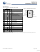
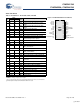
CY8C24123A CY8C24223A, CY8C24423A Ordering Information The following table lists the CY8C24x23A PSoC device’s key package features and ordering codes.
CY8C24123A CY8C24223A, CY8C24423A Document History Page Document Title: CY8C24123A, CY8C24223A, CY8C24423A PSoC® Programmable System-on-Chip™ Document Number: 38-12028 Rev. ECN Orig. of Change Submission Date Description of Change ** 236409 SFV See ECN New silicon and new document – Preliminary Data Sheet. *A 247589 SFV See ECN Changed the title to read “Final” data sheet. Updated Electrical Specifications chapter. *B 261711 HMT See ECN Input all SFV memo changes.
CY8C24123A CY8C24223A, CY8C24423A Sales, Solutions, and Legal Information Worldwide Sales and Design Support Cypress maintains a worldwide network of offices, solution centers, manufacturer’s representatives, and distributors. To find the office closest to you, visit us at cypress.com/sales. Products PSoC Clocks & Buffers PSoC Solutions psoc.cypress.com clocks.cypress.com General Low Power/Low Voltage psoc.cypress.com/solutions psoc.cypress.com/low-power Wireless wireless.cypress.