CY7C64013C CY7C64113C Full-Speed USB (12-Mbps) Function Full-Speed USB (12-Mbps) Function Cypress Semiconductor Corporation Document #: 38-08001 Rev.
CY7C64013C CY7C64113C TABLE OF CONTENTS 1.0 FEATURES .......................................................................................................................................6 2.0 FUNCTIONAL OVERVIEW ..............................................................................................................7 3.0 PIN CONFIGURATIONS ..................................................................................................................9 4.0 PRODUCT SUMMARY TABLES ....................
CY7C64013C CY7C64113C TABLE OF CONTENTS 16.6 DAC Interrupt ..........................................................................................................................31 16.7 GPIO/HAPI Interrupt ...............................................................................................................32 16.8 I2C Interrupt .............................................................................................................................32 17.0 USB OVERVIEW ........................
CY7C64013C CY7C64113C LIST OF FIGURES Figure 6-1. Clock Oscillator On-Chip Circuit ..........................................................................................17 Figure 7-1. Watchdog Reset (WDR) ......................................................................................................18 Figure 9-1. Block Diagram of a GPIO Pin ..............................................................................................19 Figure 9-2. Port 0 Data .....................................
CY7C64013C CY7C64113C LIST OF TABLES Table 4-1. Pin Assignments ..................................................................................................................10 Table 4-2. I/O Register Summary .........................................................................................................10 Table 4-3. Instruction Set Summary ......................................................................................................12 Table 9-1.
CY7C64013C CY7C64113C 1.
CY7C64013C CY7C64113C 2.0 Functional Overview The CY7C64013C and CY7C64113C are 8-bit One Time Programmable microcontrollers that are designed for full-speed USB applications. The instruction set has been optimized specifically for USB operations, although the microcontrollers can be used for a variety of non-USB embedded applications. GPIO The CY7C64013C features 19 GPIO pins to support USB and other applications.
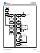
CY7C64013C CY7C64113C Logic Block Diagram 6-MHz crystal PLL 48 MHz Clock Divider 12-MHz 8-bit CPU USB SIE USB Transceiver D+[0] Upstream D–[0] USB Port 12 MHz Interrupt Controller RAM 256 byte 6 MHz 12-bit Timer 8-bit Bus PROM 8 KB GPIO PORT 0 GPIO PORT 1 P0[7:0] P1[2:0] P1[7:3] CY7C64113C only Watchdog Timer GPIO/ HAPI PORT 2 P2[0,1,7] P2[2]; Latch_Empty P2[3]; Data_Ready P2[4]; STB P2[5]; OE P2[6]; CS Power-On Reset GPIO PORT 3 DAC PORT P3[2:0] High Current Outputs P3[7:3] Additio
CY7C64013C CY7C64113C 3.
CY7C64013C CY7C64113C 4.0 Product Summary Tables 4.1 Pin Assignments Table 4-1. Pin Assignments Name I/O D+[0], D–[0] I/O 6, 7 7, 8 P0 I/O P0[7:0] 10, 14, 11, 15, 12, 16, 13, 17 P0[7:0] 11, 15, 12, 16, 13, 17, 14, 18 P1 I/O P1[2:0] 25, 27, 26 P1[2:0] 26, 4, 27 P2 I/O P2[6:2] 19, 9, 20, 8, 21 P2[6:2] 20, 10, 21, 9, 23 P3 I/O P3[2:0] 23, 5, 24 P3[2:0] 24, 6, 25 DAC I/O XTALIN 28-Pin SOIC 28-Pin PDIP 48-Pin SSOP 7, 8 Description Upstream port, USB differential data.
CY7C64013C CY7C64113C Table 4-2.
CY7C64013C CY7C64113C 4.3 Instruction Set Summary Refer to the CYASM Assembler User’s Guide for more details. Table 4-3.
CY7C64013C CY7C64113C 5.0 5.1 Programming Model 14-Bit Program Counter (PC) The 14-bit program counter (PC) allows access to up to 8 KB of PROM available with the CY7C64x13C architecture. The top 32 bytes of the ROM in the 8 Kb part are reserved for testing purposes. The program counter is cleared during reset, such that the first instruction executed after a reset is at address 0x0000h.
CY7C64013C CY7C64113C 5.1.1 Program Memory Organization after reset Address 14-bit PC 0x0000 Program execution begins here after a reset 0x0002 USB Bus Reset interrupt vector 0x0004 128-µs timer interrupt vector 0x0006 1.
CY7C64013C CY7C64113C 5.2 8-Bit Accumulator (A) The accumulator is the general-purpose register for the microcontroller. 5.3 8-Bit Temporary Register (X) The “X” register is available to the firmware for temporary storage of intermediate results. The microcontroller can perform indexed operations based on the value in X. Refer to Section 5.6.3 for additional information. 5.
CY7C64013C CY7C64113C 5.5 8-Bit Data Stack Pointer (DSP) The data stack pointer (DSP) supports PUSH and POP instructions that use the data stack for temporary storage. A PUSH instruction pre-decrements the DSP, then writes data to the memory location addressed by the DSP. A POP instruction reads data from the memory location addressed by the DSP, then post-increments the DSP. During a reset, the DSP is reset to 0x00.
CY7C64013C CY7C64113C 6.0 Clocking XTALOUT (pin 1) XTALIN (pin 2) To Internal PLL 30 pF 30 pF Figure 6-1. Clock Oscillator On-Chip Circuit The XTALIN and XTALOUT are the clock pins to the microcontroller. The user can connect an external oscillator or a crystal to these pins. When using an external crystal, keep PCB traces between the chip leads and crystal as short as possible (less than 2 cm).
CY7C64013C CY7C64113C tWATCH Last write to Watchdog Timer Register 2 ms No write to WDT register, so WDR goes HIGH Execution begins at Reset Vector 0x0000 Figure 7-1. Watchdog Reset (WDR) The USB transmitter is disabled by a Watchdog Reset because the USB Device Address Register is cleared (see Section 18.1). Otherwise, the USB Controller would respond to all address 0 transactions. It is possible for the WDR bit of the Processor Status and Control Register (0xFF) to be set following a POR event.
CY7C64013C CY7C64113C 9.0 General-Purpose I/O (GPIO) Ports VCC GPIO CFG mode 2-bits OE Q2 Q1 Control Data Out Latch Internal Data Bus 14 kΩ GPIO PIN Port Write Q3* Data In Latch Port Read STRB (Latch is Transparent except in HAPI mode) Data Interrupt Latch Control Reg_Bit Interrupt Enable *Port 0,1,2: Low Isink Port 3: High Isink Interrupt Controller Figure 9-1. Block Diagram of a GPIO Pin There are up to 32 GPIO pins (P0[7:0], P1[7:0], P2[7:0], and P3[7:0]) for the hardware interface.
CY7C64013C CY7C64113C Port 3 Data Bit # 7 6 5 4 3 Bit Name P3.7 P3.6 P3.5 P3.4 Read/Write R/W R/W R/W R/W 1 1 1 1 Reset 2 1 ADDRESS 0x03 0 P3.3 P32 P3.1 P3.0 R/W R/W R/W R/W 1 1 1 1 Figure 9-5. Port 3 Data Special care should be taken with any unused GPIO data bits. An unused GPIO data bit, either a pin on the chip or a port bit that is not bonded on a particular package, must not be left floating when the device enters the suspend state.
CY7C64013C CY7C64113C Q1, Q2, and Q3 discussed below are the transistors referenced in Figure 9-1. The available GPIO drive strength are: • Output LOW Mode: The pin’s Data Register is set to ‘0’ Writing ‘0’ to the pin’s Data Register puts the pin in output LOW mode, regardless of the contents of the Port Configuration Bits[1:0]. In this mode, Q1 and Q2 are OFF. Q3 is ON. The GPIO pin is driven LOW through Q3.
CY7C64013C CY7C64113C VCC Q1 Data Out Latch Internal Data Bus Suspend (Bit 3 of Register 0xFF) 14 kΩ DAC I/O Pin DAC Write Isink Register Internal Buffer 4 bits Isink DAC Interrupt Logic DAC Read Interrupt Enable Interrupt Polarity to Interrupt Controller Figure 10-1. Block Diagram of a DAC Pin The amount of sink current for the DAC I/O pin is programmable over 16 values based on the contents of the DAC Isink Register for that output pin.
CY7C64013C CY7C64113C Bit [4..0]: Isink [x] (x= 0..4) Writing all ‘0’s to the Isink register causes 1/5 of the max current to flow through the DAC I/O pin. Writing all ‘1’s to the Isink register provides the maximum current flow through the pin. The other 14 states of the DAC sink current are evenly spaced between these two values. Bit [7..5]: Reserved 10.2 DAC Port Interrupts A DAC port interrupt can be enabled/disabled for each pin individually.
CY7C64013C CY7C64113C Timer MSB ADDRESS 0x25 Bit # Bit Name 7 6 5 4 3 2 1 0 Reserved Reserved Reserved Reserved Timer Bit 11 Timer Bit 10 Timer Bit 9 Timer Bit 8 Read/Write - - - - R R R R Reset 0 0 0 0 0 0 0 0 Figure 11-2. Timer MSB Register Bit [3:0]: Timer higher nibble Bit [7:4]: Reserved 1.024-ms Interrupt 128- µs Interrupt 11 10 9 8 7 6 5 4 3 2 1 0 1-MHz Clock L3 L2 L1 L0 D3 D2 D1 D0 D7 D6 D5 D4 D3 D2 D1 D0 To Timer Register 8 Figure 11-3.
CY7C64013C CY7C64113C Table 12-1. HAPI Port Configuration Port Width (Bits[1:0]) HAPI Port Width 11 24 Bits: P3[7:0], P1[7:0], P0[7:0] 10 16 Bits: P1[7:0], P0[7:0] 01 8 Bits: P0[7:0] 00 No HAPI Interface Table 12-2. I2C Port Configuration 13.
CY7C64013C CY7C64113C Table 13-1. I2C Status and Control Register Bit Definitions Bit Name 2 Description 2 0 I C Enable When set to ‘1’, the I C-compatible function is enabled. When cleared, I2C GPIO pins operate normally. 1 Received Stop Reads 1 only in slave receive mode, when I2C Stop bit detected (unless firmware did not ACK the last transaction). 2 ARB Lost/Restart Reads 1 to indicate master has lost arbitration. Reads 0 otherwise.
CY7C64013C CY7C64113C to the data register before setting the Continue bit. To prevent false ARB Lost signals, the Restart bit is cleared by hardware during the restart sequence. Bit 1 : Receive Stop This bit is set when the slave is in receive mode and detects a stop bit on the bus. The Receive Stop bit is not set if the firmware terminates the I2C transaction by not acknowledging the previous byte transmitted on the I2C-compatible bus, e.g.
CY7C64013C CY7C64113C 15.0 Processor Status and Control Register Processor Status and Control Bit # 7 6 5 4 3 2 1 ADDRESS 0xFF 0 IRQ Pending Watchdog Reset USB Bus Reset Interrupt Power-On Reset Suspend Interrupt Enable Sense Reserved Run Read/Write R R/W R/W R/W R/W R R/W R/W Reset 0 0 0 1 0 0 0 1 Bit Name Figure 15-1. Processor Status and Control Register Bit 0: Run This bit is manipulated by the HALT instruction.
CY7C64013C CY7C64113C 16.0 Interrupts Interrupts are generated by the GPIO/DAC pins, the internal timers, I2C-compatible interface or HAPI operation, or on various USB traffic conditions. All interrupts are maskable by the Global Interrupt Enable Register and the USB End Point Interrupt Enable Register. Writing a ‘1’ to a bit position enables the interrupt associated with that bit position.
CY7C64013C CY7C64113C The interrupt controller contains a separate flip-flop for each interrupt. See Figure 16-3 for the logic block diagram of the interrupt controller. When an interrupt is generated, it is first registered as a pending interrupt. It stays pending until it is serviced or a reset occurs. A pending interrupt only generates an interrupt request if it is enabled by the corresponding bit in the interrupt enable registers.
CY7C64013C CY7C64113C Table 16-1. Interrupt Vector Assignments 16.2 Interrupt Vector Number ROM Address Function Not Applicable 0x0000 Execution after Reset begins here 1 0x0002 USB Bus Reset interrupt 2 0x0004 128- µs timer interrupt 3 0x0006 1.
CY7C64013C CY7C64113C 16.7 GPIO/HAPI Interrupt Each of the GPIO pins can generate an interrupt, if enabled. The interrupt polarity can be programmed for each GPIO port as part of the GPIO configuration. All of the GPIO pins share a single interrupt vector, which means the firmware needs to read the GPIO ports with enabled interrupts to determine which pin or pins caused an interrupt. A block diagram of the GPIO interrupt logic is shown in Figure 16-4. Refer to Sections 9.1 and 9.
CY7C64013C CY7C64113C 5. In master receive mode, after the master receives a byte of data: Firmware should read the data and set the ACK and Continue/Busy bits appropriately for the next byte. Clearing the MSTR MODE bit at the same time causes the master state machine to issue a stop signal to the I2C-compatible bus and leave the I2C-compatible hardware in the idle state. 6.
CY7C64013C CY7C64113C USB Status and Control Bit # 7 Bit Name ADDRESS 0 0x1F 6 5 4 3 2 1 Endpoint Size Endpoint Mode D+ Upstream D– Upstream Bus Activity Control Action Bit 2 Control Action Bit 1 Control Action Bit 0 R/W R/W R R R/W R/W R/W R/W 0 0 0 0 0 0 0 0 Read/Write Reset Figure 17-1. USB Status and Control Register Bits[2..0] : Control Action Set to control action as per Table 17-1.The three control bits allow the upstream port to be driven manually by firmware.
CY7C64013C CY7C64113C Bits[6..0] :Device Address Firmware writes this bits during the USB enumeration process to the non-zero address assigned by the USB host. Bit 7 :Device Address Enable Must be set by firmware before the SIE can respond to USB traffic to the Device Address. Bit 7 (Device Address Enable) in the USB Device Address Register must be set by firmware before the SIE can respond to USB traffic to this address.
CY7C64013C CY7C64113C Bit 6: Endpoint 0 IN Received 1= Token received is an IN token. 0= Token received is not an IN token. This bit is set by the SIE to report the type of token received by the corresponding device address is an IN token. The bit must be cleared by firmware as part of the USB processing. Bit 7: Endpoint 0 SETUP Received 1= Token received is a SETUP token. 0= Token received is not a SETUP token.
CY7C64013C CY7C64113C Bits[5..0] : Byte Count These counter bits indicate the number of data bytes in a transaction. For IN transactions, firmware loads the count with the number of bytes to be transmitted to the host from the endpoint FIFO. Valid values are 0 to 32, inclusive. For OUT or SETUP transactions, the count is updated by hardware to the number of data bytes received, plus 2 for the CRC bytes. Valid values are 2 to 34, inclusive.
CY7C64013C CY7C64113C 1. IN Token Host To Device S Y N C IN A D D R E N D P Device To Host C R C 5 D A T A 1/0 S Y N C Token Packet H O S T IN A D D R E N D P C R C 16 S Y N C A C K Hand Shake Packet Data Packet Host To Device S Y N C Data Host To Device UPDATE Device To Host C R C 5 S Y N C Token Packet NAK/STALL Data Packet UPDATE 2.
CY7C64013C CY7C64113C 19.0 USB Mode Tables Table 19-1.
CY7C64013C CY7C64113C An “Accept” in any of the columns means that the device will respond with an ACK to a valid SETUP transaction tot he host. Comments Some Mode Bits are automatically changed by the SIE in response to certain USB transactions. For example, if the Mode Bits [3:0] are set to '1111' which is ACK IN-Status OUT mode as shown in table 22-1, the SIE will change the endpoint Mode Bits [3:0] to NAK IN-Status OUT mode (1110) after ACK’ing a valid status stage OUT token.
CY7C64013C CY7C64113C the firmware recognizes the changes that the SIE might have made during the previous transaction. Note that the setup bit of the mode register is NOT locked. This means that before writing to the mode register, firmware must first read the register to make sure that the setup bit is not set (which indicates a setup was received, while processing the current USB request). This read will of course unlock the register. So care must be taken not to overwrite the register elsewhere.
CY7C64013C CY7C64113C Table 19-2.
CY7C64013C CY7C64113C 20.0 Register Summary DAC PORT ENDPOINT A3, A4 CONFIGURATION Bit 7 Bit 6 Bit 5 Bit 4 Bit 3 Bit 2 Bit 1 Bit 0 Read/Write/ Default/ Both/Reset 0x00 Port 0 Data P0.7 P0.6 P0.5 P0.4 P0.3 P0.2 P0.1 P0.0 BBBBBBBB 11111111 0x01 Port 1 Data P1.7 P1.6 P1.5 P1.4 P1.3 P1.2 P1.1 P1.0 BBBBBBBB 11111111 0x02 Port 2 Data P2.7 P2.6 P2.5 P2.4 P2.3 P2.2 P2.1 P2.0 BBBBBBBB 11111111 0x03 Port 3 Data P3.7 P3.6 P3.5 P3.4 P3.3 P3.2 P3.1 P3.
CY7C64013C CY7C64113C RESERVED Address Register Name Bit 7 Bit 6 Bit 5 Bit 4 Bit 3 Bit 2 Bit 1 Bit 0 Read/Write/ Default/ Both/Reset 0x48 Reserved Reserved Reserved Reserved Reserved Reserved Reserved Reserved Reserved Reserved 00000000 0x49 Reserved Reserved Reserved Reserved Reserved Reserved Reserved Reserved Reserved Reserved 00000000 0x4A Reserved Reserved Reserved Reserved Reserved Reserved Reserved Reserved Reserved Reserved 00000000 0x4B Reserved Res
CY7C64013C CY7C64113C 22.0 Absolute Maximum Ratings Storage Temperature ..........................................................................................................................................–65°C to +150°C Ambient Temperature with Power Applied .................................................................................................................0°C to +70°C Supply voltage on VCC relative to VSS .................................................................................
CY7C64013C CY7C64113C 23.0 Electrical Characteristics (continued) fOSC = 6 MHz; Operating Temperature = 0 to 70°C, VCC = 4.0V to 5.25V Parameter Description Conditions Min. Max. Unit 8.0 24.0 kΩ 0.1 0.3 mA DAC Interface Rup DAC Pull-up Resistance (typical 14 kΩ) Isink0(0) DAC[7:2] Sink current (0) Vout = 2.0V DC Isink0(F) DAC[7:2] Sink current (F) Vout = 2.0V DC 0.5 1.5 mA Isink1(0) DAC[1:0] Sink current (0) Vout = 2.0V DC 1.6 4.
CY7C64013C CY7C64113C tCYC tCH CLOCK tCL Figure 24-1. Clock Timing tr tr D+ 90% 90% 10% D− 10% Figure 24-2. USB Data Signal Timing Interrupt Generated Int CS (P2.6, input) tRD OE (P2.5, input) DATA (output) tOED STB (P2.4, input) D[23:0] tOEZ tOEDR (Ready) DReadyPin (P2.3, output) (Shown for DRDY Polarity=0) Internal Write Internal Addr Port0 Figure 24-3. HAPI Read by External Interface from USB Microcontroller Document #: 38-08001 Rev.
CY7C64013C CY7C64113C Interrupt Generated Int CS (P2.6, input) tWR STB (P2.4, input) tSTBZ DATA (input) D[23:0] tDSTB OE (P2.5, input) tSTBLE LEmptyPin (P2.2, output) (Shown for LEMPTY Polarity=0) (not empty) Internal Read Internal Addr Port0 Figure 24-4. HAPI Write by External Device to USB Microcontroller 25.
CY7C64013C CY7C64113C 26.0 Package Diagrams 48-Lead Shrunk Small Outline Package 51-85061-*C 28-Lead (300-Mil) PDIP SEE LEAD END OPTION 14 1 DIMENSIONS IN INCHES [MM] MIN. MAX. REFERENCE JEDEC MO-095 0.260[6.60] 0.295[7.49] 15 PACKAGE WEIGHT: 2.15 gms 28 0.030[0.76] 0.080[2.03] SEATING PLANE 1.345[34.16] 1.385[35.18] 0.290[7.36] 0.325[8.25] 0.120[3.05] 0.140[3.55] 0.140[3.55] 0.190[4.82] 0.115[2.92] 0.160[4.06] 0.015[0.38] 0.060[1.52] 0.090[2.28] 0.110[2.79] 0.009[0.23] 0.012[0.30] 0.055[1.
CY7C64013C CY7C64113C 26.0 Package Diagrams (continued) 28-Lead (300-Mil) Molded SOIC NOTE : PIN 1 ID 1. JEDEC STD REF MO-119 2. BODY LENGTH DIMENSION DOES NOT INCLUDE MOLD PROTRUSION/END FLASH,BUT 14 DOES INCLUDE MOLD MISMATCH AND ARE MEASURED AT THE MOLD PARTING LINE. 1 MOLD PROTRUSION/END FLASH SHALL NOT EXCEED 0.010 in (0.254 mm) PER SIDE 3. DIMENSIONS IN INCHES 0.291[7.39] MIN. MAX. 4. PACKAGE WEIGHT 0.85gms 0.300[7.62] 0.394[10.01] * 0.419[10.64] 15 28 PART # S28.3 STANDARD PKG. SZ28.
CY7C64013C CY7C64113C Document History Page Document Title: CY7C64013C, CY7C64113C Full-Speed USB (12 Mbps) Function Document Number: 38-08001 REV. ECN NO. Issue Date Orig.