
QDRTM-II+ SRAM 4-Word Burst Architecture (2.0 Cycle Read Latency) Specification Sheet
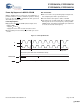
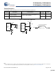
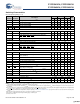
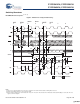
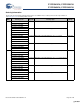
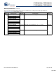
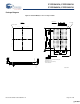
Table Of Contents
- Features
- Configurations
- Functional Description
- Selection Guide
- Logic Block Diagram (CY7C1541V18)
- Logic Block Diagram (CY7C1556V18)
- Logic Block Diagram (CY7C1543V18)
- Logic Block Diagram (CY7C1545V18)
- Pin Configuration
- Pin Definitions
- Functional Overview
- Application Example
- Write Cycle Descriptions
- Write Cycle Descriptions
- Write Cycle Descriptions
- IEEE 1149.1 Serial Boundary Scan (JTAG)
- TAP Controller State Diagram
- TAP Controller Block Diagram
- TAP Electrical Characteristics
- TAP AC Switching Characteristics
- TAP Timing and Test Conditions
- Identification Register Definitions
- Scan Register Sizes
- Instruction Codes
- Boundary Scan Order
- Power Up Sequence in QDR-II+ SRAM
- Maximum Ratings
- Operating Range
- Electrical Characteristics
- Capacitance
- Thermal Resistance
- Switching Characteristics
- Switching Waveforms
- Ordering Information
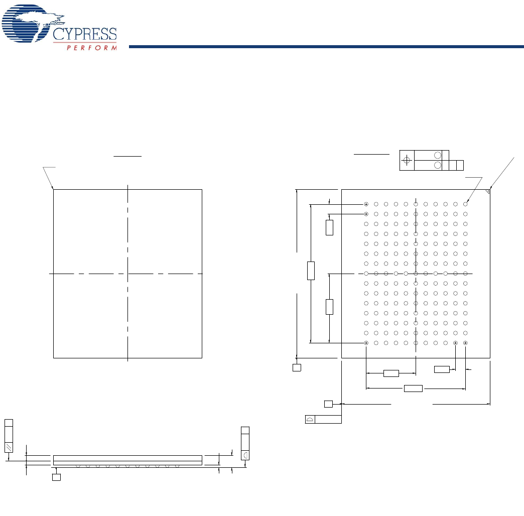
- Package Diagram
- Document History Page
CY7C1541V18, CY7C1556V18
CY7C1543V18, CY7C1545V18
Document Number: 001-05389 Rev. *F Page 27 of 28
Package Diagram
Figure 6. 165-ball FBGA (15 x 17 x 1.4 mm), 51-85195
!
0).#/2.%2
¼
¼
8
-#!"
-#
"
!
8
¼
-!8
3%!4).'0,!.%
¼
#
#
0).#/2.%2
4/06)%7
"/44/-6)%7
"
#
$
%
&
'
(
*
+
,
-
.
0
2
0
2
+
-
.
,
*
(
'
&
%
$
#
"
!
#
3/,$%20!$490%./.3/,$%2-!3+$%&).%$.3-$
./4%3
0!#+!'%7%)'(4G
*%$%#2%&%2%.#%-/$%3)'.#
0!#+!'%#/$%""!$
51-85195-*A
[+] Feedback [+] Feedback