
QDRTM-II+ SRAM 4-Word Burst Architecture (2.0 Cycle Read Latency) Specification Sheet
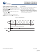
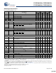
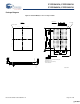
Table Of Contents
- Features
- Configurations
- Functional Description
- Selection Guide
- Logic Block Diagram (CY7C1541V18)
- Logic Block Diagram (CY7C1556V18)
- Logic Block Diagram (CY7C1543V18)
- Logic Block Diagram (CY7C1545V18)
- Pin Configuration
- Pin Definitions
- Functional Overview
- Application Example
- Write Cycle Descriptions
- Write Cycle Descriptions
- Write Cycle Descriptions
- IEEE 1149.1 Serial Boundary Scan (JTAG)
- TAP Controller State Diagram
- TAP Controller Block Diagram
- TAP Electrical Characteristics
- TAP AC Switching Characteristics
- TAP Timing and Test Conditions
- Identification Register Definitions
- Scan Register Sizes
- Instruction Codes
- Boundary Scan Order
- Power Up Sequence in QDR-II+ SRAM
- Maximum Ratings
- Operating Range
- Electrical Characteristics
- Capacitance
- Thermal Resistance
- Switching Characteristics
- Switching Waveforms
- Ordering Information
- Package Diagram
- Document History Page
CY7C1541V18, CY7C1556V18
CY7C1543V18, CY7C1545V18
Document Number: 001-05389 Rev. *F Page 24 of 28
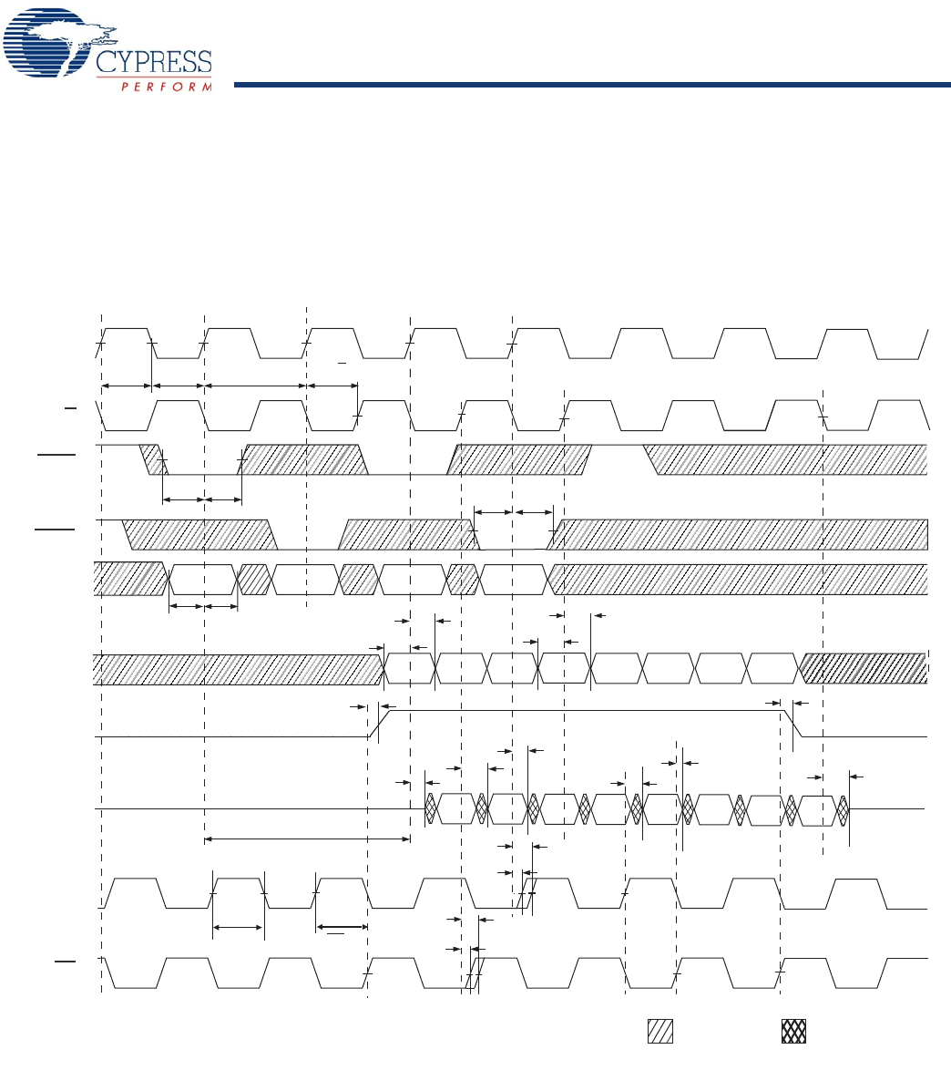
Switching Waveforms
Read/Write/Deselect Sequence
[31, 32, 33]
Figure 5. Waveform for 2.0 Cycle Read Latency
t
KH
t
KL
t
CYC
t
KHKH
NOPREAD
NOP
WRITE READ
WRITE
1
23 4 5 6
7
8
t
t
t
t
SA
HA
SC HC
t
HD
t
SC
t
HC
A0
A1
A2
A3
t
t
SD
HD
t
SD
D11D10
D12 D13 D30 D31
D32 D33
D
A
WPS
RPS
K
K
DON’T CARE UNDEFINED
CQ
CQ
t
CQOH
CCQO
t
t
CQOH
CCQO
t
t
QVLD
QVLD
t
QVLD
(Read Latency = 2.0 Cycles)
CLZ
t
t
CO
t
DOH
t
CQDOH
CQD
t
t
CHZ
Q00
Q01
Q20
Q02
Q21
Q03
Q22
Q23
t
CQH
t
CQHCQH
Q
Notes
31. Q00 refers to output from address A0. Q01 refers to output from the next internal burst address following A0, that is, A0+1.
32. Outputs are disabled (High-Z) one clock cycle after a NOP.
33. In this example, if address A2 = A1, then data Q20 = D10, Q21 = D11, Q22 = D12, and Q23 = D13. Write data is forwarded immediately as read results. This note
applies to the whole diagram.
[+] Feedback [+] Feedback