
QDRTM-II+ SRAM 4-Word Burst Architecture (2.0 Cycle Read Latency) Specification Sheet
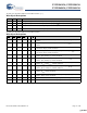
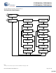
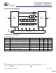
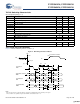
Table Of Contents
- Features
- Configurations
- Functional Description
- Selection Guide
- Logic Block Diagram (CY7C1541V18)
- Logic Block Diagram (CY7C1556V18)
- Logic Block Diagram (CY7C1543V18)
- Logic Block Diagram (CY7C1545V18)
- Pin Configuration
- Pin Definitions
- Functional Overview
- Application Example
- Write Cycle Descriptions
- Write Cycle Descriptions
- Write Cycle Descriptions
- IEEE 1149.1 Serial Boundary Scan (JTAG)
- TAP Controller State Diagram
- TAP Controller Block Diagram
- TAP Electrical Characteristics
- TAP AC Switching Characteristics
- TAP Timing and Test Conditions
- Identification Register Definitions
- Scan Register Sizes
- Instruction Codes
- Boundary Scan Order
- Power Up Sequence in QDR-II+ SRAM
- Maximum Ratings
- Operating Range
- Electrical Characteristics
- Capacitance
- Thermal Resistance
- Switching Characteristics
- Switching Waveforms
- Ordering Information
- Package Diagram
- Document History Page
CY7C1541V18, CY7C1556V18
CY7C1543V18, CY7C1545V18
Document Number: 001-05389 Rev. *F Page 19 of 28
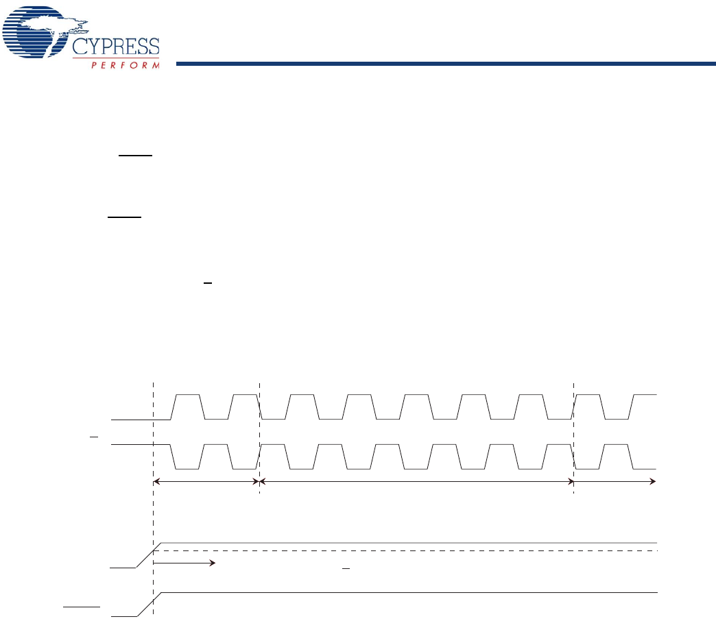
Power Up Sequence in QDR-II+ SRAM
QDR-II+ SRAMs must be powered up and initialized in a
predefined manner to prevent undefined operations. During
Power Up, when the DOFF is tied HIGH, the DLL gets locked
after 2048 cycles of stable clock.
Power Up Sequence
■ Apply power with DOFF tied HIGH (All other inputs can be
HIGH or LOW)
❐ Apply V
DD
before V
DDQ
❐ Apply V
DDQ
before V
REF
or at the same time as V
REF
■ Provide stable power and clock (K, K) for 2048 cycles to lock
the DLL.
DLL Constraints
■ DLL uses K clock as its synchronizing input. The input must
have low phase jitter, which is specified as t
KC Var
.
■ The DLL functions at frequencies down to 120 MHz.
■ If the input clock is unstable and the DLL is enabled, then the
DLL may lock onto an incorrect frequency, causing unstable
SRAM behavior. To avoid this, provide 2048 cycles stable clock
to relock to the desired clock frequency.
Figure 3. Power Up Waveforms
K
K
Fix HIGH (tie to V
DDQ
)
V
DD
/V
DDQ
DOFF
Clock Start (Clock Starts after V
DD
/V
DDQ
is Stable)
Unstable Clock > 2048 Stable Clock
Start Normal
Operation
~
~
~
~
V
DD
/V
DDQ
Stable (<
+
0.1V DC per 50 ns)
[+] Feedback [+] Feedback